
- Catalogs
- Cirrus Logic
- CS150x/160x/1601H High Efficiency Digital Power Factor Correction ICs


- Products
- Catalogs
- News & Trends
- Exhibitions
CS150x/160x/1601H High Efficiency Digital Power Factor Correction ICs

CS150x/160x/1601H High Efficiency Digital Power Factor Correction ICs
- Incorporates Digital EMI Noise Shaping and optimized digital loop compensation for enhanced efficiency with minimal external components.
- Includes comprehensive safety features such as undervoltage lockout, output overvoltage protection, input current limiting, and thermal shutdown.
- Applicable for LCD and LED TVs, monitor supplies, and battery chargers.
The CS1500 is a digital power factor correction (PFC) controller designed for universal AC input. It employs a proprietary digital algorithm for discontinuous conduction mode (DCM) with variable on-time and frequency control to achieve unity power factor. The controller is equipped with safety features for robust operation and burst mode control to minimize light-load losses.
The CS1500 features several pins for various functions, including rectifier voltage sense (IAC), link voltage sense (IFB), ground (GND), gate driver output (GD), and IC supply voltage (VDD).
- Electrical characteristics are specified for typical and minimum/maximum conditions, including supply voltage thresholds, supply current, and thermal protection.
- Absolute maximum ratings caution against operation beyond specified limits to prevent permanent damage.
Graphs illustrate the relationship between supply current, supply voltage, temperature, and other parameters, highlighting performance under various conditions.
The CS1500 is designed to replace analog PFC controllers with minimal effort. It features a unique operating frequency profile that adapts to line voltage, optimizing efficiency and performance.
The CS1500 operates in two modes: Start-up and Normal. Start-up mode is activated when the output voltage is below 90% of nominal, while Burst Mode improves efficiency under light load conditions.
The nominal output power is calculated based on efficiency, line voltage, and other parameters. The PFC output capacitor value is chosen based on voltage ripple and hold-up requirements.
Feedback control signals are used to optimize performance, with specific resistor values recommended for optimal operation.
The CS1500 includes a brownout protection feature that detects high average currents during abnormal brownout conditions. It monitors the Vrect input signal and suspends gate-drive switching when a brownout threshold is breached. The system enters standby mode during a brownout and resumes normal operation upon recovery. Hysteresis and minimum detection time are implemented to avoid erroneous detection during input transients.
The overvoltage protection (OVP) triggers immediately to stop the gate drive when the current into the IFB pin exceeds 105% of the reference current value. The IC resumes switching when the link voltage drops below a specified threshold.
If the PFC output sense resistor RIFB fails, the IC stops the gate drive when the measured output voltage is lower than the line voltage. It resumes switching when the current into the IFB pin is greater than or equal to the current into the IAC pin and Vlink exceeds the peak line voltage.
The document provides equations for calculating output power, boost inductor requirements, and sense resistor values. Key variables include efficiency (η), margin factor (α), and minimum line frequency (fline(min)).
The CS1500 is available in an 8-lead SOIC package, with a temperature range of -40°C to +125°C. The peak reflow temperature is 260°C with a moisture sensitivity level of 2.
Cirrus Logic provides this information "AS IS" without warranty. The document emphasizes that Cirrus products are not designed for critical applications involving potential risks of death or severe damage.
Catalog excerpts
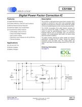
CS1500 Digital Power Factor Correction IC Features □ Digital EMI Noise Shaping □ Excellent Efficiency Under All Load Conditions □ Minimal External Devices Required □ Optimized Digital Loop Compensation □ Comprehensive Safety Features Undervoltage Lockout (UVLO) Օ Output Overvoltage Protection Input Current Limiting Օ Open/short Loop Protection for IAC & IFB Pins Thermal Shutdown Applications □ LCD and LED TVs □ Monitor Supplies □ Battery Chargers Description The CS1500 is a high-performance power factor correction (PFC) controller for universal AC input, which uses a proprietary digital algorithm for discontinuous conduction mode (DCM) with variable on-time and variable frequency control, ensuring unity power factor. The CS1500 incorporates all the safety features necessary for robust and compact PFC stages. In addition, it has burst mode control to lower the light-load/standby losses to a minimum. Protection features such as overvoltage, open- and short-circuit protection, and overtemperature help protect the device during abnormal transient conditions. The digital controller optimizes the system stability and transient performance, simplifies the PFC design, reduces the external component count and BOM costs. The simple design and minimum cost makes CS1500 the ideal choice for PFC up to 300 watts. Ordering Information See page 13. D1 TTw- <»»-- L B D2 AC Mains Vdd -O J_C3 Regulated DC Output -O CirrufLogic, Inc. @ ^ N°V "10 http://www.cirrus.com י »(AK RjgMs Resyerved) DS849F1
Open the catalog to page 1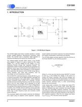
CS1500 1. INTRODUCTION Voltage 1^ R VDD Regulator POR Von v th(STP 15k IAC R 24 k J ADC Vnn R GD 15k IFB R R GND Figure 1. CS1500 Block Diagram The CS1500 digital power factor controller operates in variable on-time, variable frequency, discontinuous conduction mode (DCM). The CS1500 uses a proprietary digital algorithm to maximize the efficiency and reduce the conductive EMI. The analog-to-digital converter (ADC) shown in the CS1500 block diagram in Figure 9 is used to sense the PFC output voltage ( ) and the rectified AC line voltage ( Vrect ) by measuring currents through their respective...
Open the catalog to page 2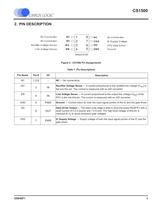
CS1500 'CIRRUS LO< 2. PIN DESCRIPTION No Connection NC [ZZ No Connection NC cz Rectifier Voltage Sense IAC [ZZ Link Voltage Sense IFB I 1 8 ZZI NC No Connection 2 1=1 VDD IC Supply Voltage 3 6 =1 GD pfc Gate Driver 4 5 l GND Ground 8-leadSOIC Figure 2. CS1500 Pin Assignments Table 1. Pin Descriptions Pin Name Pin # I/O Description NC 1,2,8 - NC ח No connections IAC 3 IN Rectifier Voltage Sense A current proportional to the rectified line voltage (Vrect) is fed into this pin. The current is measured with an A/D converter. IFB 4 IN Link Voltage Sense ח A current proportional to the output link...
Open the catalog to page 3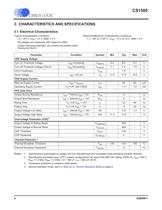
CS1500 'CIRRUS LOGIC 3. CHARACTERISTICS AND SPECIFICATIONS 3.1 Electrical Characteristics Typical characteristics conditions: Minimum/Maximum characteristics conditions: TA = 25°C, VDD = 13 V, GND = 0 V Tj = -40°to +125° C, VDD = 10 Vto 15 V, GND = 0 V All voltages are measured with respect to GND. Unless otherwise specified, all currents are positive when flowing into the IC. Parameter Condition Symbol Min Typ Max Unit VDD Supply Voltage Turn-on Threshold Voltage VDD Increasing VDD(on) 8.4 8.8 9.3 V Turn-off Threshold Voltage (UVLO) VDD Decreasing VDD(off) 7.1 7.4 7.9 V UVLO Hysteresis VHys...
Open the catalog to page 4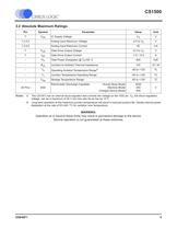
CS1500 OG/C 3.2 Absolute Maximum Ratings Pin Symbol Parameter Value Unit 7 Vdd IC Supply Voltage Vz V 1,3,4,5 - Analog Input Maximum Voltage -0.5 to Vz v 1,3,4,5 - Analog Input Maximum Current 50 mA 7 Vgd Gate Drive Output Voltage -0.3 to Vz v 7 'gd Gate Drive Output Current -1.0 / +0.5 A - Pd Total Power Dissipation @ Ta=50° C 600 mW - Junction-to-Ambient Thermal Impedance 107 °C/W - Ta Operating Ambient Temperature Range1 -40 to +125 °C - Tj Junction Temperature Operating Range -40 to +125 °C - TStg Storage Temperature Range -65 to +150 °C All Pins ESD Electrostatic Discharge Capability Human...
Open the catalog to page 5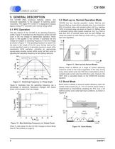
CS1500 5. GENERAL DESCRIPTION The CS1500 offers numerous features, options, and functional capabilities to the designer of switching power converters. This digital PFC control IC is designed to replace legacy analog PFC controllers with minimal design effort. 5.1 PFC Opration One key feature of the CS1500 is its operating frequency profile. Figure 11 illustrates how the frequency varies over half cycle of the line voltage in steady-state operation. When power is first applied to the CS1500, it examines the line voltage and adapts its operating frequency to the line voltage as shown in Figure...
Open the catalog to page 8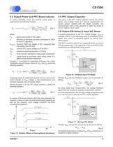
CS1500 5.4 Output Power and PFC Boost Inductor In normal operating mode, the nominal output power is estimated by the following equation. 5.5 PFC Output Capacitor The value of the PFC output capacitor should be chosen based upon voltage ripple and hold-up requirements. To ensure system stability with the digital controller, the recommended value of the capacitor is within the range of 0.5 uF/watt to 2.0 ^F/watt. 5.6 Output IFB Sense & Input IAC Sense A current proportional to the PFC output voltage, Vlink, is supplied to the IC on pin IFB and is used as a feedback control signal. This current...
Open the catalog to page 9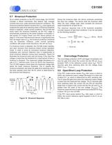
CS1500 5.7 Brownout Protection As an added protection to the PFC boost stage, the CS1500 includes a failure mechanism that detects high average currents that occur under abnormal brownout conditions. The brownout protection feature monitors the Vrect input signal and suspends the gate-drive switching when a brownout threshold breach is detected. Under normal conditions, the CS1500 will never reach the brownout threshold, as the PFC stage is automatically protected by the power limitation of Equation 2, see section 5.4 Output Power and PFC Boost Inductor on page 9. In the event that the boost...
Open the catalog to page 10
CS1500 6. SUMMARY OF EQUATIONS Eq. # Equation Variables/Recommended Values 1 Output Power (paqe 9) P _ r..n..(w .2 * Wli nk " ( W i n( mi n ) * V2) po /in(min)) * 2 * f * . * w 2 * 'max * LB* wlink P0 rated output power of the system n efficiency of the boost converter (estimated as 100% by the PFC algorithm) Vin(min) minimum RMS line voltage is 90W, measured after the rectifier and EMI filter W|ink nominal PFC output voltage must be 400 W fmax maximum switching frequency is 70 kHz |B boost inductor specified by rated power requirement a margin factor to guarantee rated output power (Po) against...
Open the catalog to page 11All Cirrus Logic catalogs and technical brochures
 Professional Service Partners
12 Pages
 CS5343/44
21 Pages
 WM0011
233 Pages
 CS4970x4
31 Pages
 CS4953xx
37 Pages
 WM9081
103 Pages
 CS42L51
84 Pages
 CS42L42
184 Pages
 CS43198
137 Pages
 CS43131
156 Pages
 CS43130
137 Pages
 CS5351
23 Pages
 CS5346
38 Pages
 CS5341/42
21 Pages
 CS35L32
51 Pages
 CS35L00/01/03
34 Pages
 Energy Measurement Brochure
13 Pages


Archived catalogs
 CS48DV2/6
2 Pages
 Mixed-Signal Audio Brochure
64 Pages






- Signal amplifying integrated circuit
- Power amplifying integrated circuit
- Compact converter
- Serial converter
- Industrial converter
- Measuring amplifier
- Voltage amplifier
- Serial receiver
- Digital amplifier
- Microcontroller
- Current amplifier
- Digital receiver
- Isolated converter
- Analog converter
- Audio amplifying integrated circuit
- Fast converter
- Video converter
- Programmable converter