- Catalogs
- CIQTEK Co., Ltd.
- Field Emission SEM5000Pro
- Company
- Products
- Catalogs
- News & Trends
- Exhibitions
Field Emission SEM5000Pro
1 /20Pages

Field Emission SEM5000Pro
1 /20Pages
Catalog excerpts

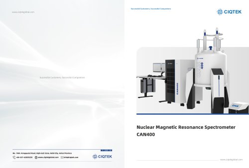
FESEM SEM5000Pro Field Emission Scanning Electron Microscope
Open the catalog to page 1
2016 CIQTEK was officially established. 2019 CIQTEK launched commercial Scanning Electron Microscope, which was recognized very well by the market. 2021 R&D overcame obstacles, and the 1st Schottky Field Emission Scanning Electron Microscope was launched. 2022 More models SEM2000, SEM3200 and SEM3300 were released, in which SEM3300 broke through the long standing resolution limit of Tungsten Filament Scanning Electron Microscope. In the same year, more than 100 units of Scanning Electron Microscopes were delivered. 2023 The High-speed SEM model HEM6000, the Focused Ion Beam Scanning Electron...
Open the catalog to page 2
Successful Customers, Successful Companions Field Emission Scanning Electron Microscope SEM5000Pro High Resolution under Low Excitation SEM5000Pro is a Schottky field emission scanning electron microscope (FE-SEM) specialized at high resolution even under low excitation voltage, with employment of an advanced facilitates crossover free beam path together with an electrostatic-electromagnetic compound lens design. These advancements reduce spatial charging effect, minimize lens aberrations, enhance imaging resolution at low voltage, achieve a resolution of 1.2 nm at 1 kV, which allows for direct...
Open the catalog to page 3
01 Low-voltage high-resolution images SEM5000&SEM5000X In-lens Electron Detector image at 200 V low excitation voltage, achieves non-destructive morphological characterization of lithium-ion polymer membrane fiber structures. In-lens Electron Detector /specimen Pore structure of SBA-15 silica-based mesoporous material characterization, In-lens Electron Detector image at 500 V low voltage without conductive coating (under dual deceleration mode with In-lens beam deceleration + Specimen stage tandem beam deceleration). In-lens Electron Detector EverhartThornley Detector ZSM-8 molecular sieve, a...
Open the catalog to page 4
Successful Customers, Successful Companions Retractable Back-Scattered Electron Detector(BSED) * Optional Retractable Back-Scattered Electron Detector(BSED) Mouse brain tissue cells/10 kV BSED-based ECCI mode (Electron Channeling Contrast Imaging) The “Electron Channeling effect” refers to a significant reduction in electron scattering by crystal lattices, when the incident electron beam satisfies the Bragg diffraction condition, allowing a large number of electrons passing through the lattice, thus exhibit a "channeling" effect. For polycrystalline materials with uniformed composition and polished...
Open the catalog to page 5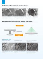
01 Simultaneously multi-channel imaging via various detectors Great resolution achieved on surface topographic features with in-lens electron detector imaging Good stereoscopic images of morphological features with Everhart-Thornley Detector imaging Atomic number contrast (Z-contrast) image with retractable BackScattered Electron Detector imaging Retractable Scanning Transmission Electron Microscopy (STEM) Detector Incident electrons Automatic insertion and retraction Multiple operating modes Bright-field (BF) imaging High-angle annular dark-field (HAADF) imaging Plant section bright-field imaging...
Open the catalog to page 6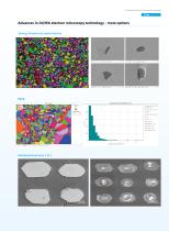
Successful Customers, Successful Companions Advances in CIQTEK electron microscopy technology - more options Energy Dispersive spectrometry
Open the catalog to page 7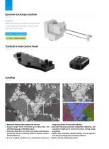
02 Specimen Exchange Loadlock * Optional Features: Effectively reduce chamber contamination Linear guiding rail design, drawer-style opening and closing 4-inches(110mmx40mm) 8-inches(208mmx40mm) Trackball & Knob Control Panel * Optional AutoMap * Optional Maximum Field of View greater than 100 mm2 Support single frame resolution up to 48k pixels, and stitched image up to 800 billion pixels Patented algorithms for local and global optimization, achieving optimal stitching effects (*Patent number: 202210372676.8) Preset imaging condition for unattended continuous image acquisition and real-time...
Open the catalog to page 8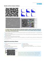
Successful Customers, Successful Companions Particle and Pore Analysis Software * Optional The software employs various target detection and segmentation algorithms, suitable for various types of particle and pore samples. It enables quantitative analysis of particle and pore statistics and can be applied in fields such as materials science, geology, and environmental science. Z Uses Mask-RCNN, an object detection and instance segmentation algorithm that accurately identifies particles in an image without the need for parameter tuning. ■ Utilizes classical watershed algorithm and ensemble contour...
Open the catalog to page 9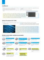
Gradient calculation for all pixels within the selected frame, enabling more precise edge detection. Multiple edge detection modes, such as line, space, and pitch. Compatibility with various image formats, including TIFF, PNG, JPG, and BMP. Built-in image post-processing functions. Automatic recognition of line width edges, resulting in more accurate measurements and higher consistency. Supports multiple edge detection modes, such as Line, Space, Pitch, etc. Compatible with multiple image formats and equipped with various commonly used image post-processing functions. The software is easy to...
Open the catalog to page 10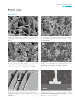
Successful Customers, Successful Companions Materials Science Nanomaterials Imaging of nickel foam with strong three-dimensional effect using a 2 kV excitation voltage with Everhart-Thornley Detector (ETD). Imaging of the distribution of platinum particles on carbon material for a common Pt-C catalyst at 2 kV voltage. Characterization of the surface features and structures of a waveguide using a low voltage (1 kV) with Everhart-Thornley Detector (ETD). Non-conductive two-dimensional material C3N4, non-destructive characterization of its fine layer structure under low-voltage conditions at 500...
Open the catalog to page 11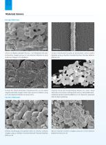
03 Materials Science Energy Materials Lithium-ion Battery Cathode Precursor - Iron Phosphate with poor conductivity, imaged using an In-lens Electron Detector (In-lens) under low voltage (1 kV) conditions. Surface SEI (Solid Electrolyte Interphase) film on the failed negative electrode imaged under high vacuum conditions using an In-lens Electron Detector (In-lens) at 3 kV. Ceramic Materials Particle morphology and growth steps on ceramic surfaces imaged using a Chamber-mounted Everhart-Thornley Detector (ETD) at 2 kV. Surface metallization quality of photovoltaic silicon wafers detected using...
Open the catalog to page 12All CIQTEK Co., Ltd. catalogs and technical brochures
 Field Emission SEM4000X
12 Pages
 Field Emission SEM4000Pro
12 Pages
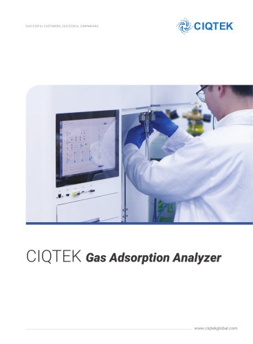 Gas Adsorption Analyzer
12 Pages
 EPR Spectrometer Modernize
6 Pages
 FIB SEMDB550
16 Pages
 Tungsten filament SEM microscope
24 Pages
- Gas analyzer
- Monitoring analyzer
- Automatic analyser
- Benchtop analyser
- Spectrometer
- Signal amplifying integrated circuit
- Generator
- Laboratory microscope
- Laboratory analyzer
- Compact analyzer
- Digital analyzer
- Laboratory spectrometer
- Inspection microscope
- LED illumination microscope
- Compact converter
- Desktop PC
- Modular PC
- Digital camera microscope
- Measuring microscope