- Catalogs
- CIQTEK Co., Ltd.
- Field emission scanning electron microscope
- Company
- Products
- Catalogs
- News & Trends
- Exhibitions
Field emission scanning electron microscope
1 /24Pages
Field emission scanning electron microscope
1 /24Pages
Catalog excerpts

Field Emission Scanning Electron Microscope
Open the catalog to page 1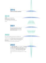
2016 CIQTEK was officially established. CIQTEK launched commercial Scanning Electron Microscope, which was recognized very well by the market. Schottky Field Emission Scanning Electron Microscope was launched. More models SEM2000, SEM3200 and SEM3300 were released, in which SEM3300 broke through the long standing resolution limit of Tungsten Filament Scanning Electron Microscope. In the same year, more than 100 units of Scanning Electron Microscopes were delivered. The High-speed SEM model HEM6000, the Focused Ion Beam Scanning Electron Microscope (FIB-SEM) model DB500 and Ultra-high Resolution...
Open the catalog to page 2
Successful Customers, Successful Companions Field Emission Scanning Electron Microscope Extensions and Software PI 2-14
Open the catalog to page 3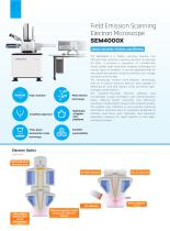
Field Emission Scanning Electron MicroscopeSEM4000XStable, Versatile, Flexible, and Efficient. The SEM4000X is a stable, versatile, flexible, and efficient field emission scanning electron microscope (FE-SEM). It achieves a resolution of [email protected], easily tackles high-resolution imaging challenges for various types of samples. It can be upgraded with an ultra beam deceleration mode to enhance low-voltage resolution even further. The microscope utilizes multi-detector technology, with an in-column electron detector (UD) capable of detecting SE and BSE signals while providing high-resolution...
Open the catalog to page 4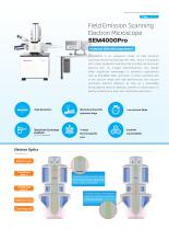
Successful Customers, Successful Companions Successful Customers, Successful Companions Field Emission Scanning Electron MicroscopeSEM4000ProAnalytical SEM with Large Beam I SEM4000Pro is an analytical model of field emission scanning electron microscope (FE-SEM), which is equipped with a high-brightness and long-life Schottky field emission electron gun. Its 3-stage electromagnetic lens design offers significant advantages in analytical applications such as EDS,EBSD, WDS, and more. It comes standard with a low vacuum mode and high-performance low vacuum secondary electron detector, as well as...
Open the catalog to page 5
Under low-vacuum mode, a range of 10-180 Pa can be reached without a pressure limiting aperture. The specially designed objective lens vacuum chamber minimizes the electron mean free path in low vacuum condition, achieves resolution of 1.5 nm at 30 kV under low vacuum mode. The secondary electron emission from the specimen surface ionizes air molecules, generates electrons, ions, and photons simultaneously. The generated electrons further on ionize other air molecules, low-vacuum secondary electron detector (LVD) captures a large amount of photon signals produced in such process Gas molecules...
Open the catalog to page 6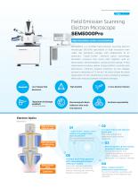
Successful Customers, Successful Companions Successful Customers, Successful Companions Field Emission Scanning Electron MicroscopeSEM5000Pro High Resolution under Low Excitation SEM5000Pro is a Schottky field emission scanning electron microscope (FE-SEM) specialized at high resolution even under low excitation voltage, with employment of an advanced "Super-Tunnel" electron optics technology, facilitates crossover free beam path together with an electrostatic-electromagnetic compound lens design. These advancements reduce spatial charging effect, minimize lens aberrations, enhance imaging resolution...
Open the catalog to page 7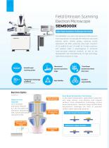
Field Emission Scanning Electron MicroscopeSEM5000XUltra-high resolution challenges the limits The SEM5000X is an ultra-high resolution field emission scanning electron microscope (FE-SEM) with optimized electron optics column design, reducing overall aberrations by 30%, achieving ultra-high resolution of 0.6 nm@l 5 kV and 1.0 nm@1 kV. Its high resolution and stability make it advantageous in advanced nano-structural materials research, as well as the development and manufacturing of high technology node semiconductor 1C chips. Objective lens Upgrade Lens chromatic aberration reduced by 12%,...
Open the catalog to page 8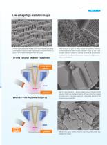
Successful Customers, Successful Companions In-lens Electron Detector image at 200 V low excitation voltage, achieves non-destructive morphological characterization of lithium-ion polymer membrane fiber structures. Pore structure of SBA-15 silica-based mesoporous material characterization, In-lens Electron Detector image at 500 V low voltage without conductive coating (under dual deceleration mode with In-lens beam deceleration + Specimen stage tandem beam deceleration). ZSM-8 molecular sieve, a typical catalyst across multiple frontier research field. Low-voltage imaging without conductive coating...
Open the catalog to page 9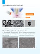
Retractable Back-Scattered Electron Detector (BSED) BSED-based ECCI mode (Electron Channeling Contrast Imaging) The "Electron Channeling effect" refers to a significant reduction in electron scattering by crystal lattices, when the incident electron beam satisfies the Bragg diffraction condition, allowing a large number of electrons passing through the lattice, thus exhibit a "channeling" effect. For polycrystalline materials with uniformed composition and polished flat surfaces, the intensity of backscattered electrons relies on the relative orientation between the incident electron beam and...
Open the catalog to page 10
Successful Customers, Successful Companions Successful Customers, Successful Companions Great resolution achieved on Good stereoscopic images of Atomic number contrast (Z-contrast) surface topographic features with morphological features with image with retractable Back- in-lens electron detector imaging Everhart-Thornley Detector imaging Scattered Electron Detector imaging Multiple operating modes Bright-field (BF) imaging Dark-field (DF) imaging High-angle annular dark-field (HAADF) imaging Atomic number contrast (Z-contrast) image with Retractable Back-Scattered Electron Detector Plant section...
Open the catalog to page 11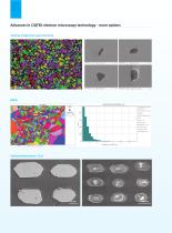
Advances in CIQTEK electron microscopy technology - more options
Open the catalog to page 12
Specimen Exchange Loadlock * Optional Effectively reduce chamber contamination Linear guiding rail design, drawer-style opening and closing ■ Maximum Field of View greater than 100 mm2 ■ Support single frame resolution up to 48k pixels, and stitched image up to 800 billion pixels ■ Patented algorithms for local and global optimization, achieving optimal stitching effects ('Patent number: 202210372676.8) ■ Preset imaging condition for unattended continuous image acquisition and real-time stitching ■ Automatic focusing, automatic astigmatism deduction, and automatic brightness & contrast functions...
Open the catalog to page 13All CIQTEK Co., Ltd. catalogs and technical brochures
 Field Emission SEM4000X
12 Pages
 Field Emission SEM4000Pro
12 Pages
 Field Emission SEM5000Pro
20 Pages
 Gas Adsorption Analyzer
12 Pages
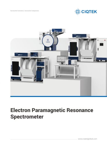
 EPR Spectrometer Modernize
6 Pages
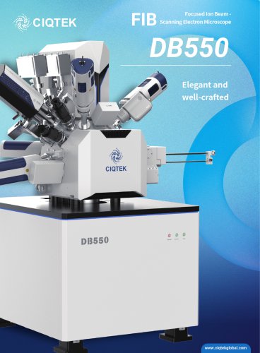 FIB SEMDB550
16 Pages
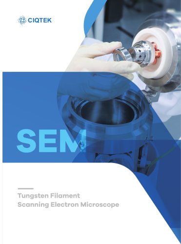 Tungsten filament SEM microscope
24 Pages
- Gas analyzer
- Monitoring analyzer
- Automatic analyser
- Benchtop analyser
- Spectrometer
- Signal amplifying integrated circuit
- Generator
- Laboratory microscope
- Laboratory analyzer
- Compact analyzer
- Digital analyzer
- Laboratory spectrometer
- Inspection microscope
- LED illumination microscope
- Compact converter
- Desktop PC
- Modular PC
- Digital camera microscope
- Measuring microscope