- Catalogs
- CIQTEK Co., Ltd.
- FIB SEMDB550
- Company
- Products
- Catalogs
- News & Trends
- Exhibitions
FIB SEMDB550
1 /16Pages
FIB SEMDB550
1 /16Pages
Catalog excerpts
ICIQTEK FIB Focused Ion Beam -Scanning Electron Microscope
Open the catalog to page 1
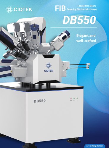
DB550 is a Field Emission Scanning Electron Microscope with Focused Ion Beam column for nano-analysis and specimen preparation, which is applied with "Super Tunnel" electron optics technology-low aberration and magnetic-free objective lens design, with "Low-voltage & FHigh-resolution" ability that ensures its nano-scale analytical capability. The ion column facilitates a Ga+ liquid metal ion source with highly stable and high quality ion beam to ensure nano-fabrication capability. DB550 is equipped with an integrated nano-manipulator, gas injection system, and a user-friendly GUI software, which...
Open the catalog to page 2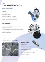
Focused Ion Beam Colurnj^- Resolution: 3 nm@30 KV Probe current: 1 pA~65 nA Accelerating voltage range: 0.5 KV-30 kV Ion source exchange interval: >1000 hours Stability: 72 hours uninterrupted operation Chamber internally mounted Three-axis all-piezoelectric driven motion accuracy: <10 nm Maximum travel speed: 2 mm/s Integrated control system Ion Beam-Electron Beam Collaboration wGas Injection System^ Single GIS design Various gas precursor sources available Needle insertion distance: >35 mm Motion repeatability: <10 pm Heating temperature control repeatability: <0.1 °C Heating range: room temperature...
Open the catalog to page 3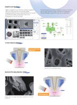
Highly integrated user interface platform together with scanning electron microscope (SEM) Imaging and processing integrated within an overall user interface with comparative references displayed on the left and right Self-developed accessories hardware and user interface such as gas injection system and nano-manipulator, intuitive design of layout for easy-to-use operation In-lens electron detector Everhart-Thornley Detector (ETD)
Open the catalog to page 4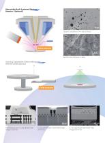
Scanning Transmission Electron Microscopy detector (STEM, Optional) Advanced process 1C chips Bright-field image (STEM-BF) 1C Chip device layer Dark-field image (STEM-DF) 1C Chip aluminum layer Dark-field image (STEM-DF)
Open the catalog to page 5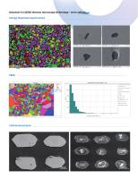
Advances in CIQTEK electron microscopy technology - more options
Open the catalog to page 6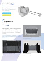
Specimen Exchange Loadlock wFeatures:_ Effectively reduce chamber contamination Linear guiding rail design, drawer-style opening and closing In the semiconductor industry, 1C chips may encounter various failures. To improve reliability, various methods are used to analyze the chips. Among them, Focused Ion Beam (FIB) analysis is a reliable analytical technique.
Open the catalog to page 7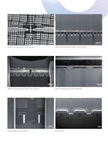
28nm Cu Processed 1C Chip Top view 28nm Cu Processed 1C Chip/ Cross-Section
Open the catalog to page 8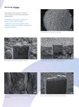
Observation and analysis of material cross-sections for research and process development Morphologyl observation/particle size analysis/cross-section analysis Composition and phase analysis/failure analysis of lithium-ion battery material/TEM sample preparation...
Open the catalog to page 9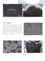
Ceramic materialg^ Material analysis: The FIB-SEM system can perform high-precision micro-nano machining and imaging to ceramic materials, combined with various signal detection modes such as backscattered electrons (BSE), energy-dispersive X-ray spectroscopy (EDX), Electron Backscattered Diffraction Pattern (EBSD), and secondary ion mass spectrometry (SIMS), to study the material in a micro to nano-scale with three-dimensional space in depth.
Open the catalog to page 10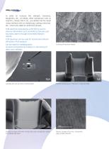
Alloy material In order to increase the strength, hardness, toughness, etc., of metals, other substances such as ceramics, metals, fibers, etc., are added into the metal using methods such as metallurgy, casting, extrusion, etc., which are called its reinforced phases. TEM specimen prepared by a FIB-5EM is used to observe information such as reinforced phases and boundary atoms through transmitted electron signals. TEM specimen can be used for transmission Kikuchi Diffraction (TKD) analysis. Can be used for metallographic analysis/compositional analysis/in-situ testing of alloy cross-sections
Open the catalog to page 11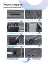
Machining capab Rough then precision milling for gross preparation of lamella (7) Lamella thinning process (4) Once welded, finish-off of a U-cut prior to lamella lift-out. (5) Lift-out done by a nano-manipulator
Open the catalog to page 12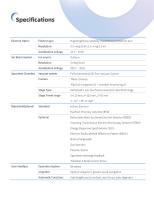
Electron Optics Electron gun High Brightness Schottky Field Emission Electron Gun Ion Beam System Ion source Gallium Specimen Chamber Vacuum system Fully Automated, Oil-Free Vacuum System Camera Three cameras (Optical navigation XI + chamber monitoringx2) Stage Type Motorized 5-axis mechanical eucentric specimen stage Stage Travel range X=110 mm, Y=110 mm, Z=65 mm Detector&Optional Standard In-lens Electron Everhart-Thornley Detector(ETD) Optional Retractable Back-Scattered Electron Detector(BSED) Scanning Transmission Electron Microscopy Detector (STEM) Energy Dispersive Spectrometer (EDS) Electron...
Open the catalog to page 14
Successful Customer's, Successful Campanians Email: [email protected] Website: www.ciqtekgiobai.com Address: No. 1969, Kongquetai Road, High-tech Zone, Hefei City, Anhui Province, China
Open the catalog to page 16All CIQTEK Co., Ltd. catalogs and technical brochures
 Field Emission SEM4000X
12 Pages
 Field Emission SEM4000Pro
12 Pages
 Field Emission SEM5000Pro
20 Pages
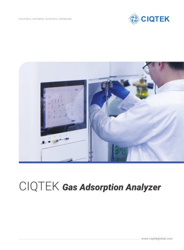 Gas Adsorption Analyzer
12 Pages
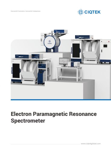
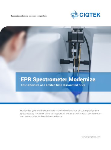 EPR Spectrometer Modernize
6 Pages
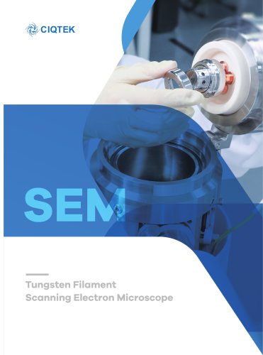 Tungsten filament SEM microscope
24 Pages
- Gas analyzer
- Monitoring analyzer
- Automatic analyser
- Benchtop analyser
- Signal amplifying integrated circuit
- Generator
- Laboratory microscope
- Laboratory analyzer
- Compact analyzer
- Digital analyzer
- Laboratory spectrometer
- Inspection microscope
- LED illumination microscope
- Compact converter
- Desktop PC
- Modular PC
- Digital camera microscope
- Measuring microscope