- Catalogs
- Chotest Technology Inc.
- White Light Interferometry Probe SuperView WX100
- Company
- Products
- Catalogs
- News & Trends
- Exhibitions
White Light Interferometry Probe SuperView WX100
1 /2Pages

White Light Interferometry Probe SuperView WX100
1 /2Pages
Catalog excerpts

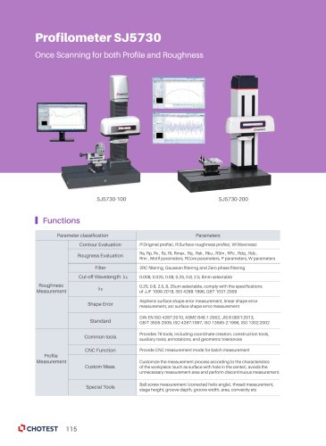
White Light Interferometry Probe SuperView WX100 White Light Interferometry Probe In-line roughness and 3D profile inspection Semiconductor, polished silicon wafer, thin silicon wafer, wafer IC 3C electronics, sapphire glass roughness, metal shell mold defects, glass screen height difference Double anti-collision protection Software ZSTOP and hardware electronic sensors.Besides it could accept external anti-collision electronic signals. Four DOF motorized tilt Provides an electric tilt adjustment design with four degrees of freedom in pitch and yaw, which greatly reduces the manufacturing difficulty of the customer's measuring stage. Capable to measure samples with different height. Users need not to prepare a moving Z axis SDK Provide the software package for customers to carry out secondary development, so that customers can develop the software program to control the probe for automatic measurement and analysis. Functions Measurement function: it can realize high precision Z scanning of sample surface and obtain 3D image. Analysis function: It can obtain 2D and 3D data such as surface roughness, micro-nano-level contour Light Source Video System Objective Lens Lens Turret Single hole / 3 holes manual Roughness RMS Repeatability*1 Step Height Measurement Note: *1 Measure Sa 0.2nm silicon wafer in a laboratory environment according to the ISO 25178. *2 Measure standard 5μm steps height block in a laboratory environment according to the ISO 10610-1:2009. size, etc. Programming function: Support pre-configured data processing and analysis tool steps, one-click to complete the whole process from measurement to analysis. Batch analysis: Data processing and analysis templates can be customized according to the customer demands, and one-click batch analysis can be realized for the same type of parameter data.
Open the catalog to page 1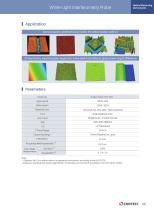
Optical Measuring Instruments I ApplicationSemiconductor, polished silicon wafer, thin silicon wafer, wafer IC 3C electronics, sapphire glass roughness, metal shell mold defects, glass screen height difference I Parameters Model No. *1 Measure Sa 0.2nm silicon wafer in a laboratory environment according to the ISO 25178. *2 Measure standard 5|jm steps height block in a laboratory environment according to the ISO 10610-1:2009.
Open the catalog to page 2All Chotest Technology Inc. catalogs and technical brochures
 PRODUCT CATALOGUE
67 Pages
 WR50 Rotary Axis Clibrator
4 Pages
 WD4000 SERIES
4 Pages
 PO40 PO40L PO60
2 Pages
 SJ5800-100 SJ5800-200
4 Pages
 SJ5900-100 SJ5900-200
4 Pages
 VX1060 VX1100
1 Page
 Laser Interferometer SJ6000
4 Pages
 Profilometers SJ57 Series
8 Pages
 Profilometer SJ5700 Series
4 Pages


- Test machine
- Top ozono measuring system
- Microscope
- Calibration system
- Automated testing machine
- Optical microscope
- Industrial testing machine
- Vertical testing machine
- Laboratory microscope
- Laboratory testing machine
- Digital gauge
- Portable gauge
- Precision testing machine
- Top ozono industrial measuring instrument
- Top ozono automatic measuring system
- Top ozono optical measuring system
- Inspection microscope
- Precision calibration equipment
- Inspection machine