
- Catalogs
- Chotest Technology Inc.
- Unpatterned Wafer 3D Inspection System-WD4000-WD4200


- Company
- Products
- Catalogs
- News & Trends
- Exhibitions
Unpatterned Wafer 3D Inspection System-WD4000-WD4200
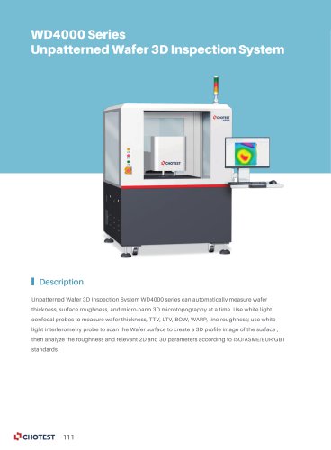
Unpatterned Wafer 3D Inspection System-WD4000-WD4200
The WD4000 Series Unpatterned Wafer 3D Inspection System is designed to automatically measure wafer thickness, surface roughness, and micro-nano 3D microtopography. It utilizes white light confocal probes for measuring thickness, TTV, LTV, BOW, WARP, and line roughness, and white light interferometry to create a 3D profile image of the wafer surface. The system analyzes roughness and relevant 2D and 3D parameters according to ISO/ASME/EUR/GBT standards.
This system is used in professional inspection settings to reconstruct the 3D shape of wafers through non-contact measurement. It provides stable calculations for thickness, roughness, and total thickness variation (TTV). During wafer thinning processes, surface roughness Sa values are critical for evaluating processing quality, with fine grinding silicon wafers showing a roughness Sa value around 5nm and a repeatability of 0.046987nm.
- Wafer Sizes: 4", 6", 8", 12"
- Measurement Parameters: Thickness, TTV, LTV, BOW, warp, flatness, line roughness
- Sensor: High-precision white light confocal sensors
- Measuring Range: 100μm~2000μm
- Accuracy: ±0.25μm
- Repeatability: 0.2μm
- Resolution: 25nm
- Light Source: White LED
- Objective Lens: 10X (2.5X, 5X, 20X, 50X optional)
- Field of View: 0.96 mm×0.96 mm
- Overall Size: 1500×1500×2000mm
- Weight: About 1500kg
- Working Environment: Temp. 20°C±1°C/hour, RH 30~80%
- Roughness performance is measured using SQ parameters for a 0.2nm SA silicon wafer in a laboratory environment according to ISO 25178.
- Step height performance is measured using a standard 4.7μm stage block according to ISO 5436-1: 2000.
Catalog excerpts
Unpatterned Wafer 3D Inspection System WD4000 Series Unpatterned Wafer 3D Inspection System Professional Inspection Equipment Application Thickness and warpage measurement for unpatterned wafer Description Unpatterned Wafer 3D Inspection System WD4000 series can automatically measure wafer thickness, surface roughness, and micro-nano 3D microtopography at a time. Use white light confocal probes to measure wafer thickness, TTV, LTV, BOW, WARP, line roughness; use white light interferometry probe to scan the Wafer surface to create a 3D profile image of the surface , then analyze the roughness and relevant 2D and 3D parameters according to ISO/ASME/EUR/GBT Measurement results of wafer thickness and warpage The 3D shape based on the upper and lower surfaces of the wafer is reconstructed by non-contact measurement. The powerful measurement and analysis software ensures the stable calculation for the thickness, roughness, total thickness variation(TTV) of the wafer.
Open the catalog to page 1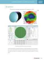
Unpatterned Wafer 3D Inspection System WD4000 Series Unpatterned Wafer 3D Inspection System Professional Inspection Equipment Application Thickness and warpage measurement for unpatterned wafer Description Unpatterned Wafer 3D Inspection System WD4000 series can automatically measure wafer thickness, surface roughness, and micro-nano 3D microtopography at a time. Use white light confocal probes to measure wafer thickness, TTV, LTV, BOW, WARP, line roughness; use white light interferometry probe to scan the Wafer surface to create a 3D profile image of the surface , then analyze the roughness and...
Open the catalog to page 2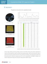
Unpatterned Wafer 3D Inspection SystemI ApplicationRoughness measurement for unpatterned wafer Thinned silicon wafer rough grinding silicon wafer fine grinding silicon wafer Multi-file analysis of 25 times measurement data for fine grinding wafer During rough grinding and fine grinding process for the Wafer thinning, the surface roughness Sa values and their stability are used to evaluate the processing quality. When the thinned silicon wafer is measured in the strong noise environment of the production workshop, the roughness Sa values of the fine grinding silicon wafers are ranging around 5nm,...
Open the catalog to page 3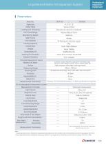
Unpatterned Wafer 3D Inspection System| Parameters Model No. Thickness Measurement System Arsenide, nitride, phosphorus, germanium, phosphorurate, lithium crickets, sapphire, si [icon, silicon carbide, glass, etc. High-precision white light confocal sensors Measuring Range Scanning Path Measurement Parameters Full map area scanning, Union Jack path, free multi-point Thickness, TTV (Total thickness variation), LTV, BOW, warp, flatness, line roughness 3D microtopography Measurement System *1 Roughness performance is obtained by measuring SQ parameters for a 0.2nm SA silicon wafer in the laboratory...
Open the catalog to page 4All Chotest Technology Inc. catalogs and technical brochures
 PRODUCT CATALOGUE
67 Pages
 WR50 Rotary Axis Clibrator
4 Pages
 WD4000 SERIES
4 Pages
 PO40 PO40L PO60
2 Pages
 SJ5800-100 SJ5800-200
4 Pages
 SJ5900-100 SJ5900-200
4 Pages
 VX1060 VX1100
1 Page
 Laser Interferometer SJ6000
4 Pages
 Profilometers SJ57 Series
8 Pages
 Profilometer SJ5700 Series
4 Pages











- Test machine
- Chotest measuring instrument
- Chotest measuring system
- Microscope
- Calibration system
- Automated testing machine
- Optical microscope
- Industrial testing machine
- Vertical testing machine
- Laboratory microscope
- Laboratory testing machine
- Digital gauge
- Precision testing machine
- Portable gauge
- Chotest industrial measuring instrument
- Chotest automatic measuring system
- Inspection microscope
- Desktop microscope
- Quality control testing machine
- Inspection machine