- Catalogs
- Chotest Technology Inc.
- SuperView WT3000 | WT3200 3D Hybrid Optical Profilometer
- Company
- Products
- Catalogs
- News & Trends
- Exhibitions
SuperView WT3000 | WT3200 3D Hybrid Optical Profilometer
1 /2Pages
SuperView WT3000 | WT3200 3D Hybrid Optical Profilometer
1 /2Pages
Catalog excerpts
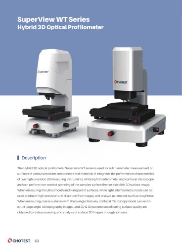
3D Optical Surface Profilometer SuperView WT Series Hybrid 3D Optical Profilometer Technical Parameters Adding W-Ultra high-speed scanning module can increase scanning speed by several times. Model Light Source Video System Interference Objective Lens Confocal Objective Lenses Standard Field of View Lens Turret Motorized 5-hole turret Size Travel Range XY Object Table Load Capacity Control Mode Tilt Travel Range Control Mode Z stroke scanning Range Surface Topography Repeatability STR*1 0.1nm (White light interferometry) 0.005nm (White light interferometry) Accuracy: 0.5%; Repeatability: 0.1% (1σ) (White light interferometry) The Hybrid 3D optical profilometer Superview WT series is used for sub nanometer measurement of surfaces of various precision components and materials. It integrates the performance characteristics of two high-precision 3D measuring instruments, white light interferometer and confocal microscope, and can perform non-contact scanning of the samples surface then re-establish 3D surface image. When measuring the ultra smooth and transparent surfaces, white light interferometry mode can be used to obtain high-precision and distortion-free images, and analyze parameters such as roughness. When measuring coarse surfaces with sharp angle features, confocal microscopy mode can recon- Operating Environment 0.6Mpa oil-free and water-free, 6mm diameter of hose Power Supply No strong magnetic field, no corrosive gas struct large angle 3D topography images, and 2D & 3D parameters reflecting surface quality are obtained by data processing and analysis of surface 3D images through software. Note: *1 Use EPSl mode to measure Sa 0.2nm silicon wafer in the laboratory environment; Single stripe, 80um filter for full field of view *2 Measure Sa 0.2nm silicon wafer in a laboratory environment according to the ISO 25178 *3 Measure standard 5μm steps height block in a laboratory environment according to the ISO 10610-1:2009 *4 When the software noise evaluation is 4nm≤3σ≤10nm, the Roughness RMS repeatability is revised down to 0.015nm, the Step height measurement accuracy is revised down to 0.7%, and the step height measurement repeatability is revi
Open the catalog to page 1
Optical Measuring Instruments 3D Optical Surface ProfilometerI Technical ParametersAdding W-Ultra high-speed scanning module can increase scanning speed by several times. Model *1 Use EPSl mode to measure Sa 0.2nm silicon wafer in the laboratory environment; Single stripe, 80um filter for full field of view *2 Measure Sa 0.2nm silicon wafer in a laboratory environment according to the ISO 25178 *3 Measure standard 5pm steps height block in a laboratory environment according to the ISO 10610-1:2009 *4 When the software noise evaluation is 4nm<3o<10nm, the Roughness RMS repeatability is revised...
Open the catalog to page 2All Chotest Technology Inc. catalogs and technical brochures
 PRODUCT CATALOGUE
67 Pages
 WR50 Rotary Axis Clibrator
4 Pages
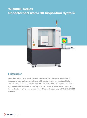
 WD4000 SERIES
4 Pages
 PO40 PO40L PO60
2 Pages
 SJ5800-100 SJ5800-200
4 Pages
 SJ5900-100 SJ5900-200
4 Pages
 VX1060 VX1100
1 Page
 Laser Interferometer SJ6000
4 Pages
 Profilometers SJ57 Series
8 Pages
 Profilometer SJ5700 Series
4 Pages


- Test machine
- Top ozono measuring system
- Calibration system
- Automated testing machine
- Optical microscope
- Industrial testing machine
- Vertical testing machine
- Laboratory microscope
- Laboratory testing machine
- Digital gauge
- Portable gauge
- Precision testing machine
- Top ozono industrial measuring instrument
- Top ozono automatic measuring system
- Top ozono optical measuring system
- Inspection microscope
- Precision calibration equipment
- Inspection machine