
- Catalogs
- Chotest Technology Inc.
- Patterned Wafer Critical Dimension & Overlay Measurement System BOKI_1000


- Company
- Products
- Catalogs
- News & Trends
- Exhibitions
Patterned Wafer Critical Dimension & Overlay Measurement System BOKI_1000

Patterned Wafer Critical Dimension & Overlay Measurement System BOKI_1000
Catalog excerpts
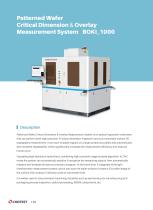
Critical Dimension & Overlay Measurement System Patterned Wafer Critical Dimension & Overlay Measurement System BOKI_1000 Professional Inspection Equipment Overlay Offset Measurement During wafer manufacturing, the offset of the overlay after photoetching process is measured in Photo area, exposure of wafer, and compensation values based on the measurement are imported into the lithography machine to optimize the stability of the wafer photoetching process. Description Patterned Wafer Critical Dimension & Overlay Measurement System is an optical inspection instrument that can perform both high-precision XY plane dimension inspection and sub-nanometer surface 3D topography measurement. It can scan multiple regions on a large surface accurately and automatically with excellent repeatability, which significantly increases the measurement efficiency and reduces human error. Equipping high-resolution optical lens, combining high-precision image analysis algorithm, in CNC mode the system can automatically position & recognize the measuring objects, then automatically measure and evaluate all sizes according to program. At the same time, it integrates white light interferometry measurement system, which can scan the wafer surface to create a 3D profile image of Key Dimensions Measurement During wafer manufacturing, it requires to control critical dimensions of Die in multiple processes, and SuperView automatically extracts the feature edges of Die, and at the same time it measures all features according to program efficiently and accurately. the surface, then analyze Z-direction sizes in nanometer level. It is widely used in ultra-precision machining industries such as semiconductor manufacturing and packaging process inspection, optical processing, MEMS components, etc.
Open the catalog to page 1
Critical Dimension & Overlay Measurement System Patterned Wafer Critical Dimension & Overlay Measurement System BOKI_1000 Professional Inspection Equipment Overlay Offset Measurement During wafer manufacturing, the offset of the overlay after photoetching process is measured in Photo area, exposure of wafer, and compensation values based on the measurement are imported into the lithography machine to optimize the stability of the wafer photoetching process. Description Patterned Wafer Critical Dimension & Overlay Measurement System is an optical inspection instrument that can perform both high-precision...
Open the catalog to page 2
Professional Inspection Equipment Critical Dimension & Overlay Measurement System Critical Dimension & Overlay Measurement System 4 pcs of Cassette, size is customizable Feeding Sensor With anti-skid function Light Source White/Green LED (single or double is optional) Barcode Scanner Barcode recognition Video System Micro Objective Lens Interferometric Objective Lens 3D Dimensions Measurement During wafer manufacturing, it is necessary to measure the bottom width of the grooves to check whether the distance between dies is qualified after the previous process in Photo area. The software automatically...
Open the catalog to page 3
Professional Inspection Equipment Critical Dimension & Overlay Measurement System Critical Dimension & Overlay Measurement System 4 pcs of Cassette, size is customizable Feeding Sensor With anti-skid function Light Source White/Green LED (single or double is optional) Barcode Scanner Barcode recognition Video System Micro Objective Lens Interferometric Objective Lens 3D Dimensions Measurement During wafer manufacturing, it is necessary to measure the bottom width of the grooves to check whether the distance between dies is qualified after the previous process in Photo area. The software automatically...
Open the catalog to page 4All Chotest Technology Inc. catalogs and technical brochures
 PRODUCT CATALOGUE
67 Pages
 WR50 Rotary Axis Clibrator
4 Pages
 WD4000 SERIES
4 Pages
 PO40 PO40L PO60
2 Pages
 SJ5800-100 SJ5800-200
4 Pages
 SJ5900-100 SJ5900-200
4 Pages
 VX1060 VX1100
1 Page
 Laser Interferometer SJ6000
4 Pages
 Profilometers SJ57 Series
8 Pages
 Profilometer SJ5700 Series
4 Pages













- Test machine
- Chotest measuring instrument
- Chotest measuring system
- Microscope
- Automated testing machine
- Calibration system
- Optical microscope
- Industrial testing machine
- Vertical testing machine
- Laboratory microscope
- Laboratory testing machine
- Digital gauge
- Precision testing machine
- Portable gauge
- Chotest industrial measuring instrument
- Chotest automatic measuring system
- Inspection microscope
- Desktop microscope
- Quality control testing machine
- Inspection machine