
- Catalogs
- Bruker Optics GmbH & Co. KG
- QUANTAX EBSD

- Company
- Products
- Catalogs
- News & Trends
- Exhibitions
QUANTAX EBSD
QUANTAX EBSD
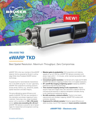
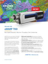
eWARP TKD is a cutting-edge detector from Bruker, designed for nanomaterials characterization in scanning electron microscopes (SEM) using an on-axis geometry. It excels in sensitivity, speed, spatial resolution, and data integrity, setting new standards in orientation and phase mapping of nanomaterials.
- Productivity: Achieves acquisition and indexing speeds up to 5,700 fps, providing orientation and phase maps within 1-5 minutes.
- Spatial Resolution: Offers mapping with better than 2 nm spatial resolution when combined with a high-end FE-SEM.
- Imaging Speed: DF- and BF-like imaging enabled by patented on-chip binning technology.
- Time-Resolved Mapping: Capable of capturing real-time microstructural evolution during in-situ experiments.
- Minimal Artifacts: Low beam requirements and ultrafast mapping eliminate the need for drift correction.
- Delicate Sample Handling: Extreme signal efficiency allows for low-dose, low-kV TKD mapping of beam-sensitive materials.
- Detection Method: CMOS/Direct Electron Detection
- Active Area: 26 x 26 mm2 silicon sensor
- Pixel Size: 160 x 160 µm2
- Dynamic Range: 15 bit (91db)
- Operating Conditions: Accelerating voltage range of 2 kV – 30 kV, probe current < 2 nA
- Pixel Resolution: Native 162 x 162 pixels, binned 18x18 pixels
- Minimum Integration Time: 175 µs /10 µs
- Radiation Hardening: Expected lifetime of at least 15,000 hours at 30 kV
- Cooling System: Active - Peltier
The eWARP TKD demonstrates superior performance in nanomaterials characterization. An orientation map (IPFz) was acquired from a 15 nm gold thin film with a 2 nm step size. The map size was 4.3 Mpixels, covering an area of 5.1 µm x 3.9 µm, with a pixel size of 2 nm. The indexing rate was 92.5%, and the speed was 2873 patterns/second, resulting in a total map time of 25:13 minutes. The accelerating voltage was 30 kV, and the probe current was 2 nA. The analysis identified 108,506 grains smaller than 50 nm, with a mean equivalent grain diameter of 21.2 nm.
eWARP TKD offers unmatched performance for researchers and engineers working on nanomaterials, providing high-speed, high-resolution mapping with minimal artifacts and excellent data integrity.
Catalog excerpts
eWARP TKD Best Spatial Resolution. Maximum Throughput. Zero Compromise. eWARP TKD is the new member of the eWARP detector family, powered by Bruker’s cutting edge Wide Area Pixelated (WARP) sensor technology. Massive gains in productivity: With acquisition and indexing Purpose-built for nanomaterials characterization in the SEM using the “on-axis” geometry, eWARP TKD outperforms existing solutions across all key metrics, e.g., sensitivity, speed, spatial resolution and data integrity. The groundbreaking signal efficiency and speed of eWARP TKD set new standards in the orientation and phase mapping of nanomaterials. Featuring a new, larger pixelated sensor with a resolution of 162 x 162 pixels and an active area exceeding 26 x 26 mm2 , eWARP TKD delivers a powerful set of advantages for researchers and engineers working on nanomaterials: Innovation with Integrity speeds of up to 5,700 fps, eWARP TKD delivers orientation and phase maps within 1 - 5 minutes, while maintaining excellent data quality and integrity. Unmatched spatial resolution: Combined with a high-end FE-SEM eWARP TKD delivers mapping at better than 2 nm spatial resolution. DF- and BF-like imaging at lightning speed: Enabled by eWARP’s patented on-chip binning technology. Time resolved mapping during in-situ experiments: Rapidly acquire maps and images every few seconds to capture real-time microstructural evolution in electron-transparent samples during in-situ heating and mechanical testing. No drift correction, minimal artifacts: Thanks to low beam requirements and ultrafast mapping, eWARP TKD renders drift correction obsolete. Engineered for delicate samples: Extreme signal efficiency enables low-dose, low-kV TKD mapping for beam-sensitive materials.
Open the catalog to page 1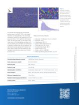
Figure 1 Orientation map (IPFz) acquired from a gold thin film sample and corresponding crystal size dis50 nm tribution and stats. Please note that no data cleaning was applied and that “crystals” with less than 5 pixels were excluded from the histogram and statistics. Map size: 4.3 Mpixels / 5.1 µm x 3.9 µm Pixel size: 2 nm Indexing rate: 92.5 % Speed: 2873 patterns/second Total map time: 25:13 min Accelerating voltage: 30 kV Probe current: 2 nA Grains < 50 nm: 108,506 Mean equivalent grain diameter: 21.2 nm Technical Specifications Chip technology/Detection method CMOS/Direct Electron Detection...
Open the catalog to page 2All Bruker Optics GmbH & Co. KG catalogs and technical brochures
 ELIO
8 Pages
 heliX+
2 Pages
 HI 90
2 Pages
 SIGIS 2
12 Pages
 EM 27/SUN Series
8 Pages
 EM 27
2 Pages
 OPS
8 Pages
 MATRIX-MF II
2 Pages
 TANGO II
5 Pages
 MATRIX-F II
16 Pages
 BEAM
8 Pages
 MOBILE-IR II
12 Pages
 INVENIO
12 Pages
 ALPHA II
12 Pages
 BRAVO
12 Pages
 LUMOS II
8 Pages
 OMEGA 5
8 Pages
 MATRIX II-MG Series
8 Pages
Archived catalogs
 MPA III
7 Pages
- Gas analyzer
- Concentration analyzer
- Monitoring analyzer
- Automatic analyser
- Benchtop analyser
- Bruker spectrometer
- Process analyzer
- Gas detector
- Continuous analyzer
- Real-time analyzer
- Laboratory microscope
- Laboratory analyzer
- Digital analyzer
- Compact analyzer
- Infrared analyser
- Temperature analyzer
- Laboratory spectrometer
- Inspection microscope
- In-line analyzer