AMMP-6333
1 /10Pages

AMMP-6333
1 /10Pages
Catalog excerpts
AMMP-6333 18-GHz to 33-GHz, 0.2-W Driver Amplifier in SMT Package Data Sheet Description The AMMP-6333 is a broadband 0.2-W driver amplifier designed for use in transmitters operating in various frequency bands from 18 GHz to 33 GHz. This small, easy-to-use device provides over 23 dBm of output power (P-1dB) and more than 20 dB of gain at 25 GHz. It was optimized for linear operation with an output power at the third order intercept point (OIP3) of 30 dBm. The AMMP-6333 features a temperature compensated RF power detection circuit that enables power detection sensitivity of 0.3 V/W at 25GHz. It is fabricated using Broadcom's unique 0.25-m E-mode PHEMT technology, which eliminates the need for negative gate biasing voltage. Features ■ Frequency range: 18 GHz to 33 GHz ■ Small signal gain: 20 dB ■ P-1dB: 23 dBm ■ Return loss (in/out): -10 dB Applications ■ Microwave radio systems ■ Satellite VSAT, up/down link ■ LMDS and Pt-Pt mmW long haul ■ Broadband wireless access (including 802.16 and 802.20 WiMax) ■ WLL and MMDS loops Functional Block Diagram NOTE MSL Rating = Level 2A
Open the catalog to page 1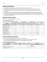
Data Sheet Electrical Specifications ■ Small/large-signal data measured in a fully de-embedded test fixture form Ta = 25°C. ■ Pre-assembly into package performance verified 100 percent on-wafer per AMMC-6220 published specifications. ■ This final package part performance is verified by a functional test correlated to actual performance at one or more frequencies. ■ Specifications are derived from measurements in a 50Q test environment. Aspects of the amplifier performance may be improved over a more narrow bandwidth by application of additional conjugate, linearity, or low noise (opt) matching. ■...
Open the catalog to page 2
Data Sheet Table 3 Thermal Properties a. Operation in excess of any one of these conditions may result in permanent damage to this device.
Open the catalog to page 3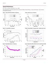
Data Sheet Typical Performance (TA = 25°C, Vd =5V, IdQ = 230 mA, Zin = Zout = 50) (Data obtained from a test fixture with 2.4-mm connectors. Effects of the test fixture—losses and mismatch—have not been removed from the dat.a) Figure 1 Gain and Reverse Isolation vs. Frequency Figure 2 Return Loss vs. Frequency Figure 4 Typical IMD3 vs. Frequency (SCL = Single Carrier Level) Figure 5 Typical Noise Figure vs. Frequency Figure 6 Output Power, PAE, and Drain Current vs. Input Power at 30 GHz
Open the catalog to page 4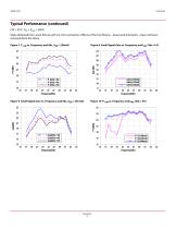
Data Sheet Typical Performance (continued) (TA = 25°C, Zin = Zout = 50) (Data obtained from a test fixture with 2.4-mm connectors. Effects of the test fixture—losses and mismatch—have not been removed from the dat.a) Figure 7 P-1dB vs. Frequency and Vds, (IdQ = 230mA) Figure 8 Small Signal Gain vs. Frequency and IdQ, (Vds =5 V) Figure 9 Small Signal Gain vs. Frequency and Vds, (IdQ = 230 mA)
Open the catalog to page 5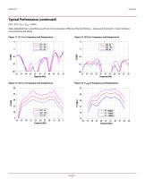
Data Sheet Typical Performance (continued) (TA = 25°C, Zin = Zout = 50) (Data obtained from a test fixture with 2.4-mm connectors. Effects of the test fixture—losses and mismatch—have not been removed from the dat.a) Figure 11 |S11| vs. Frequency and Temperature Figure 12 |S22| vs. Frequency and Temperature Figure 13 |S21| v.s Frequency and Temperature Figure 14 P-1dB vs Frequency and Temperature
Open the catalog to page 6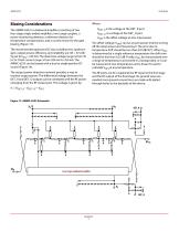
Data Sheet Biasing Considerations Where: VDET_R is the voltage at the DET_R port The AMMP-6333 is a balanced amplifier consisting of two four-stage single-ended amplifiers, two Lange couplers, a power monitoring detector, a reference detector for temperature compensation, and a current mirror for the gate biasing (Figure 15). VDET_O is a voltage at the DET_O port VOFS is the offset voltage at zero input power The recommended quiescent DC bias conditions for optimum gain, output power, efficiency, and reliability are: Vd = 5V with Vg set for IdQ = 230 mA. The drain bias voltage range is from 3V...
Open the catalog to page 7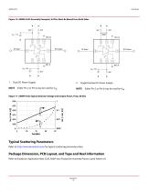
Data Sheet Figure 16 AMMP-6333 Assembly Examples, Vd Pins Must Be Biased from Both Sides Dual DC Power Supply Single Positive DC Power Supply Figure 17 AMMP-6333 Typical Detector Voltage and Output Power, Freq=30 GHz Typical Scattering Parameters Refer to http://www.broadcom.com for typical scattering parameters data. Package Dimension, PCB Layout, and Tape and Reel information Refer to Broadcom Application Note 5520, AMxP-xxxx Production Assembly Process (Land Pattern A).
Open the catalog to page 8
Data Sheet Table 5 Ordering Information
Open the catalog to page 9
For product information and a complete list of distributors, please go to our web site: www.broadcom.com. Broadcom, the pulse logo, Connecting everything, Avago Technologies, Avago, and the A logo are among the trademarks of Broadcom and/or its affiliates in the United States, certain other countries and/or the EU. Copyright © 2014-2017 by Broadcom. All Rights Reserved. The term "Broadcom" refers to Broadcom Limited and/or its subsidiaries. For more information, please visit www.broadcom.com. Broadcom reserves the right to make changes without further notice to any products or data herein to...
Open the catalog to page 10All Broadcom catalogs and technical brochures
 BROCADE SX6 EXTENSION BLADE
8 Pages
 AMMC-5040
13 Pages
 Product brochure
15 Pages

Archived catalogs
 2009 Product Brochure
9 Pages
 BCM2004
2 Pages
 Broadcom - Product Brochure
9 Pages
- Bourn And Koch display
- Bourn And Koch network switch
- Bourn And Koch rotary encoder
- Bourn And Koch incremental encoder
- Bourn And Koch proximity sensor
- Managed switch
- Bourn And Koch absolute rotary encoder
- LED display panel
- Diode
- Single-turn rotary encoder
- Bourn And Koch transistor
- Multi-turn rotary encoder
- Rectangular proximity sensor
- High-resolution rotary encoder
- GNSS receiver
- Numeric display
- 7-segment display
- 24 ports network switch
- Low-noise amplifier
- SMT diode