AMMC-5040
1 /13Pages

AMMC-5040
1 /13Pages
Catalog excerpts
AMMC-5040 20-GHz to 45-GHz GaAs Amplifier Data Sheet The AMMC-5040 is a high gain broadband amplifier designed for both military applications and commercial communication systems. This four-stage amplifier has input and output matching circuitry for use in 50- environments. It is fabricated using PHEMT integrated circuit structures that provide exceptional broadband performance. The backside of this chip is both RF and DC ground. This simplifies the assembly process and reduces assembly related performance variations and costs. For improved reliability and moisture protection, the die is passivated at the active areas. This MMIC is a cost effective alternative to hybrid (discrete-FET) amplifiers that require complex tuning and assembly process. Chip Size: Chip Size Tolerance: ±10 μm (±0.4 mils) Chip Thickness: Frequency range: 20 GHz–45 GHz High gain: 25 dB Gain flatness: ±1.5 dB Return loss: Broadband gain block Broadband driver amplifier Point-to-point radio LMDS EW Instru
Open the catalog to page 1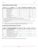
Data Sheet a. Measured in wafer form with Tchuck = 25°C (except 9ch-bsJ
Open the catalog to page 2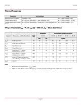
Data Sheet NOTE 1. Data measured in wafer form, Tchuck = 25°C. 2. 100% on-wafer RF test is done at frequency = 24 GHz, 27 GHz, 29 GHz, 37 GHz, and 40 GHz, except as noted.
Open the catalog to page 3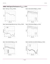
Data Sheet AMMC-5040 Typical Performance (Tchuck = 25°C) Figure 1 Gain, VDD = 4.5 V, IDD = 300 mA Figure 2 Gain and Drain Voltage, IDD = 300 mA 35 Figure 3 Input and Output Return Loss, VDD = 4.5V, IDD = 300 mA Figure 4 Gain and Drain Voltage, IDD = 350 mA 30 Figure 5 Gain and Drain Voltage, IDD = 4.5V Figure 6 Input Return Loss and Drain Voltage, IDD = 350 mA 0 -5 INPUT RETURN LOSS (dB)
Open the catalog to page 4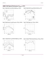
Data Sheet AMMC-5040 Typical Performance (Tchuck = 25°C) Figure 7 Output Return Loss and Drain Voltage, IDD = 350 mA Figure 8 Output Power (P-1dB) and Drain Current, VDD = 4.5V 25 OUTPUT RETURN LOSS (dB) Figure 9 Output Power at P-1dB and P-3dB, VDD = 4.5V, IDD = 300 mA Figure 10 Noise Figure, VDD = 4.5V, IDD = 300 mA Figure 11 Output Power (P-1dB) and Drain Voltage, IDD = 300 mA Figure 12 Output 3rd Order Intercept Point, VDD = 4.5V, IDD = 300 mA
Open the catalog to page 5
Data Sheet NOTE T = 25°C. See Frequency Multiplier Biasing and Operation for bias conditions for operation as a multiplier.
Open the catalog to page 6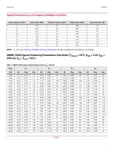
Data Sheet Typical Performance as a X3 Frequency Multiplier (See Note) T = 25°C. See Frequency Multiplier Biasing and Operation for bias conditions for operation as a multiplier. AMMC-5040 Typical Scattering Parameters (See Note) (Tchuck = 25°C, VDD = 4.5V, IDD = 300 mA, Zin = Zout = 50) Table 1 AMMC-5040 Typical Scattering Parameters, IDD = 300 mA S11
Open the catalog to page 7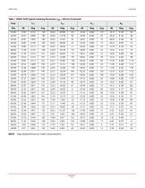
Data Sheet Table 1 AMMC-5040 Typical Scattering Parameters, IDD = 300 mA (Continued) S11
Open the catalog to page 8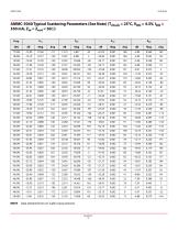
Data Sheet AMMC-5040 Typical Scattering Parameters (See Note) (Tchuck = 25°C, VDD = 4.5V, IDD = 350 mA, Zin = Zout = 50) S11
Open the catalog to page 9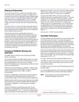
Data Sheet Biasing and Operation The recommended DC bias condition for the AMMC-5040 is with all four drains connected to a single 4.5V supply and all four gates connected to an adjustable negative voltage supply as shown in Figure 15. The gate voltage is adjusted for a total drain supply current of typically 300 mA. Figure 1 thorugh Figure 12 can be used to help estimate the minimum drain voltage and current necessary for a given RF gain and output power. As shown in Figure 13, the second, third, and fourth stage DC drain bias lines are connected internally and therefore require only a single...
Open the catalog to page 10
Data Sheet Figure 13 AMMC-5040 Simplified Schematic Diagram Vd1 Matching Matching Matching Figure 14 AMMC-5040 Bonding Pad Locations (Dimensions in Microns) 1442 1175 543 432
Open the catalog to page 11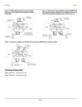
Data Sheet Figure 15 AMMC-5040 Assembly for Normal Amplifier Applications with Single Drain and Single Gate Supply Connections To V DD DC Drain Supply ≥100 pF Gold Plated Shim (Optional) Figure 16 Separate First-stage Gate Bias for Using the AMMC-5040 as a Frequency Doubler or Quadrupler. This diagram also shows an option to the Vg2 jumper bonding scheme used in Figure 15. To V DD DC Drain Supply RFin RFout Vg2 to Vg3 jumper (or use separate Vg2 bond as shown in Figure 16) Figure 17 Separate First-stage Gate and Drain Bias for Using the AMMC-5040 as a Fequency Tripler To Vd1 DC Drain Supply RFin...
Open the catalog to page 12
For product information and a complete list of distributors, please go to our web site: www.broadcom.com. Broadcom, the pulse logo, Connecting everything, Avago Technologies, Avago, and the A logo are among the trademarks of Broadcom and/or its affiliates in the United States, certain other countries and/or the EU. Copyright © 2010-2017 by Broadcom. All Rights Reserved. The term "Broadcom" refers to Broadcom Limited and/or its subsidiaries. For more information, please visit www.broadcom.com. Broadcom reserves the right to make changes without further notice to any products or data herein to...
Open the catalog to page 13All Broadcom catalogs and technical brochures
 BROCADE SX6 EXTENSION BLADE
8 Pages
 AMMP-6333
10 Pages
 Product brochure
15 Pages

Archived catalogs
 2009 Product Brochure
9 Pages
 BCM2004
2 Pages
 Broadcom - Product Brochure
9 Pages
- Bourn And Koch display
- Bourn And Koch network switch
- Bourn And Koch rotary encoder
- Bourn And Koch incremental encoder
- Bourn And Koch proximity sensor
- Managed switch
- Bourn And Koch absolute rotary encoder
- LED display panel
- Diode
- Single-turn rotary encoder
- Bourn And Koch transistor
- Multi-turn rotary encoder
- Rectangular proximity sensor
- High-resolution rotary encoder
- GNSS receiver
- Numeric display
- 7-segment display
- 24 ports network switch
- Low-noise amplifier
- SMT diode