
- Catalogs
- Avago Technologies
- HSMP-389D PIN Diode Diversity Switch

HSMP-389D PIN Diode Diversity Switch

HSMP-389D PIN Diode Diversity Switch
The HSMP-389D is a cost-effective and low-loss diversity switch designed for operation between 50MHz and 6GHz. It features a unique 4 PIN diode configuration and is housed in a compact SOT-143 package, ideal for space-constrained applications. Key performance metrics at 900MHz include an insertion loss (IL) of -0.36dB, isolation (ISO) of -24.72dB, input third-order intercept point (IIP3) of 55.35dBm, and input 1dB compression point (IP1dB) of 46.25dBm. It is suitable for wireless applications like DECT phones, wireless LAN, and WiMAX.
- Unique configurations in Surface Mount SOT-143 for increased flexibility, board space saving, and cost reduction.
- Low distortion switching and low capacitance.
- Low Failure In Time (FIT) rate.
- Specifications at 900MHz with IF=5mA: Low IL (0.36dB), High ISO (24.72dB), High power handling (IP1dB, 46.25dBm), High linearity (IIP3, 55.35dBm).
At a case temperature of +25°C, the maximum ratings include a forward current of 1A, peak inverse voltage of 100V, junction temperature of 150°C, and storage temperature range from -65 to 150°C. The thermal resistance is 500°C/W.
At +25°C, each diode has a breakdown voltage of 128V, forward voltage between 0.90V and 1.10V, and typical series resistance of 4.50 Ohms at 100MHz and 1mA. The total capacitance is between 0.50pF and 0.65pF at 1MHz and 0V reverse voltage.
At nominal operating conditions (Tc = +25°C, IF = 5mA), the IIP3 is 55.35dBm at 0.9GHz, 56.24dBm at 1.9GHz, and 57.69dBm at 2.4GHz. The IP1dB is 46.25dBm at 0.9GHz, 46.80dBm at 1.9GHz, and 47.40dBm at 2.4GHz.
Figures illustrate the relationships between forward current and voltage, RF resistance and forward bias current, total capacitance and reverse voltage, and return loss, insertion loss, and isolation versus frequency.
The truth table provides control voltage configurations for low loss paths between RF ports.
The HSMP-389D is available in bulk or tape and reel packaging, with specific part numbers for different quantities. The package outline and recommended PCB pad layout are provided for assembly guidance.
Catalog excerpts
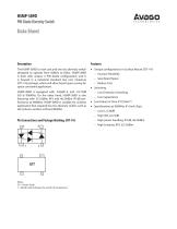
HSMP-389D PIN Diode Diversity Switch Data Sheet The HSMP-389D is a low cost and low loss diversity switch designed to operate from 50MHz to 6GHz. HSMP-389D is built with unique 4 PIN diode configuration, and it is housed in a industrial standard low cost miniature SOT-143 package, which will allow board space saving for space constraint application. • Unique configurations in Surface Mount SOT-143 HSMP-389D is equipped with -0.36dB IL and -24.72dB ISO @ 900MHz. On the other hand, HSMP-389D is also featuring with 55.35dBm IIP3 and 46.25dBm IP1dB performance @ 900MHz. HSMP-389D is suitable for wireless application that required low loss diversity switch, such as dect phone, wireless LAN and WiMAX. – Increase Flexibility – Save Board Space – Reduce Cost • Switching – Low Distortion Switching – Low Capacitance • Low Failure In Time (FIT) Rate [1] • Specifications at 900MHz; IF=5mA (Typ.) – Low IL, 0.36dB – High ISO, 24.72dB Pin Connections and Package Marking, SOT-143 3 Notes: G7 = Device Code ? = Month code indicates the month of manufacture – High power handling, IP1dB, 46.25dBm – High Linearity, IIP3, 55.35dBm
Open the catalog to page 1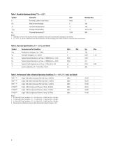
Table 1. Absolute Maximum Rating Nl Tc = +25°C Symbol Parameter Units Absolute Max. IF Forward Current (1u,s Pulse) Amp 1 Piv Peak Inverse Voltage V 100 TSTG Storage Temperature °C -65 to 150 1. Operation in excess of anyone of these conditions may result in permanent damage to the device. 2. Tc = 25°C, Tc where is defined to be the temperature at the package pins where contacts is made to the circuit board. Table 2. Electrical Specifications, Tc = +25°C, each diode Symbol Parameterand Test Condition Units Min. Typ Max. VBR Breakdown Voltage © lR= IOUA V - 128 Rs Typical Series Resistance @ Freq...
Open the catalog to page 2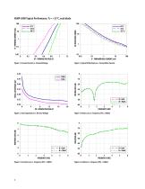
HSMP-389D Typical Performance, Tc = +25°C, each diode 100 25°C 125°C -50°C Figure 3. Total Capacitance vs. Reverse Voltage Figure 4. Return Loss vs. Frequency (Pin = 0dBm) Figure 5. Insertion Loss vs. Frequency (Pin = 0dBm) 0.1 1 10 IF - FORWARD BIAS CURRENT (mA) Figure 2. Typical RF Resistance vs. Forward Bias Current Figure 1. Forward Current vs. Forward Voltage Figure 6. Isolation vs. Frequency (Pin = 0dBm)
Open the catalog to page 3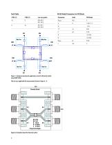
Truth Table APLAC Model Parameters for PIN Diode Figure 7. A diagram showing the application circuit for Diversity Switch using HSMP-389D. This set-up is applicable for measurement shown in Figure 4 – 6. 30.0 Diversity Switch RO 4350 DK 3.48 RF 1 H 10 mil RF 2 W 0.56mm G 0.44mm Avago Technologies Figure 8. Evaluation Board for Diversity Switch
Open the catalog to page 4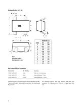
XXX-package marking Part Number Ordering Information Part Number No. of Devices Container HSMP-389D-TR1 3000 Tape & Reel, per 7" Reel HSMP-389D-TR2 10000 Tape & Reel, per 13" Reel TapeandReelingconformstoElectroniclndustriesRS-481, For lead-free option, the part number will have the "Taping of Surface Mounted Components for Automated character "G" at the end, eg. -TR2G for a 10K pc lead-free Placement". reel.
Open the catalog to page 5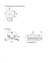
Recommended PCB Pad Layout for AVAGO's SOT-143 Products Device Orientation COVER TAPE Note: "AB" represents package marking code. "C" represents date code.
Open the catalog to page 6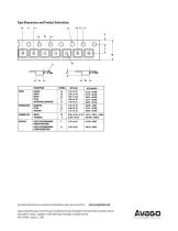
Tape Dimensions and Product Orientation For product information and a complete list of distributors, please go to our web site: www.avagotech.com Avago, Avago Technologies, and the A logo are trademarks of Avago Technologies in the United States and other countries. Mk « — ^m Data subject to change. Copyright © 2005-2009 Avago Technologies. All rights reserved. (3
Open the catalog to page 7All Avago Technologies catalogs and technical brochures
 AFCD-V84LP
1 Page
 BCM4778
2 Pages
 AFBR-57H5MZ
29 Pages
 ASMB-UTF0-0D20B
12 Pages
 ASMT-YTD7-0AA02
15 Pages
 ASMT-YTC7-0AA02
15 Pages
 ASMT-RF45-AN002
8 Pages
 Optical Sensor
64 Pages


Archived catalogs
 WLAN Low-Noise Amplifier
10 Pages
 Optoisolation Products
58 Pages
 125 Megabaud Versatile Link
12 Pages
 LED Solutions
96 Pages


- Display module
- Angular encoder
- Incremental encoder
- Incremental rotary encoder
- Switching relay
- Absolute rotary encoder
- Signal amplifying integrated circuit
- Electronic display panel
- Optical rotary encoder
- Transceiver module
- Electronic filter
- Magnetic rotary encoder
- Power amplifying integrated circuit
- Visible LED
- Transistor module
- Solid state relay
- GNSS receiver
- Ethernet transceiver
- Rectifier diode