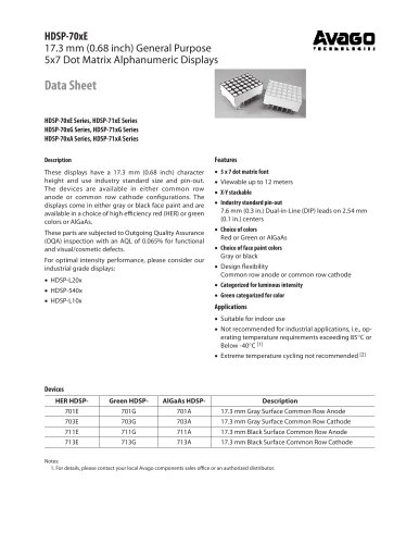
Catalog excerpts
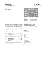
Data Sheet Chip Size: Chip Size Tolerance: Chip Thickness: Pad Dimensions: 930 x 630 µm (36.6 x 24.8 mils) ±10 µm (±0.4 mils) 100 ± 10 µm (4 ± 0.4 mils) 80 x 80 µm (3.2 x 3.2 mils) Avago’s AMMC-2008 is a monolithic PHEMT SPDT switch with low insertion loss and high isolation from DC to 50 GHz. This MMIC is designed for general-purpose applications. For improved reliability and moisture protection, the die is passivated at the active areas. One series and two shunt PHEMTs per throw provide 2.0 dB insertion loss and 28 dB isolation at 40 GHz. • Wide frequency range: DC – 50 GHz Absolute Maximum Ratings [1] Symbol Parameters/Conditions Storage Temperature Note: 1. Operation in excess of any one of these conditions may result in permanent damage to this device. • Single pole double throw switch • Low insertion loss: 2.3 dB (max.) at 40 GHz • High isolation: 25 dB (min.) at 40 GHz • Medium input power: P-1dB: +14 dBm Applications • Communications • Radar • ECM • EW • Fiber optics • Pulse modulation • Port isolation • Transfer switching • High speed switching • Replacement of mechanical switches
Open the catalog to page 1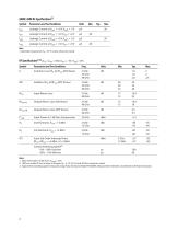
AMMC-2008 DC Specifications[1] Symbol Parameters and Test Conditions Note: 1. Backside temperature Tb = 25°C unless otherwise noted. Parameters and Test Conditions IL Insertion Loss, RFin to RFout (ON throw) ISO Isolation, RFin to RFout (OFF throw) RLin Input Return Loss RLout-on Output Return Loss (ON throw) RLout-off Output Return Loss (OFF throw) Input Power at 1 dB Gain Compression Input 3rd Order Intercept Point, dBm RFin1=RFin2 = +5 dBm, ∆f = 2 MHz Control Switching Speed[3] 10% – 90% rise time 90% – 10% fall time Notes: 1. Data measured in wafer form, Tchuck= 25°C. 2. 100% on-wafer...
Open the catalog to page 2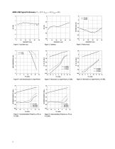
AMMC-2008 Typical Performance (T = 25°C, VseM = -3V, Vse,2 = OV) Figure 1. Insertion Loss. Figure 8. Intermodulation Products vs. Pin at
Open the catalog to page 3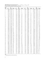
AMMC-2008 Typical Scattering Parameters[1] (Tchuck = 25°C, Vsel1 = -3 V, Vsel2 = 0 V) RF Out1: OFF (terminated in 50-ohms), RF Out2: ON Freq. GHz dB Note: 1. Data obtained from on-wafer measurements.
Open the catalog to page 4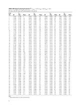
AMMC-2008 Typical Scattering Parameters[1] (Tchuck = 25°C, Vsel1 = 0V, Vsel2 = -3V) RF Out1: ON, RF Out2: OFF (terminated in 50-ohms) Freq. GHz dB Note: 1. Data obtained from on-wafer measurements.
Open the catalog to page 5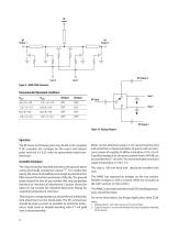
Recommended Operation Conditions Vsel1 Figure 10. Biasing Diagram. Operation The RF Input and Output ports may be DC or AC-coupled. If DC‑coupled, the voltages on the Input and Output ports must be 0 ± 0.25 volts for guaranteed switch performance. Assembly Techniques Mesh can be attached using a 2 mil round tracking tool and a tool force of approximately 22 grams with an ultrasonic power of roughly 55 dB for a duration of 76 ± 8 mS. A guided wedge at an ultrasonic power level of 64 dB can be used for the 0.7 mil wire. The recommended wire bond stage temperature is 150 ± 2°C. The chip should...
Open the catalog to page 6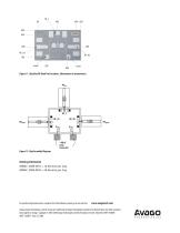
Figure 11. Chip Bias/RF Bond Pad Locations. (dimensions in micrometers) Figure 12. Chip Assembly Diagram. Ordering Information AMMC-2008-W10 = 10 devices per tray AMMC-2008-W50 = 50 devices per tray For product information and a complete list of distributors, please go to our web site: Avago, Avago Technologies, and the A logo are trademarks of Avago Technologies Limited in the United States and other countries. Data subject to change. Copyright © 2005-2008 Avago Technologies Limited. All rights reserved. Obsoletes 5989-3928EN AV02-1260EN - June 23, 2008
Open the catalog to page 7All Avago Technologies catalogs and technical brochures
-
AFCD-V84LP
1 Pages
-
BCM4778
2 Pages
-
AFBR-57H5MZ
29 Pages
-
ASMB-UTF0-0D20B
12 Pages
-
ASMT-YTD7-0AA02
15 Pages
-
ASMT-YTC7-0AA02
15 Pages
-
ASMT-RF45-AN002
8 Pages
-
Optical Sensor
64 Pages
Archived catalogs
-
WLAN Low-Noise Amplifier
10 Pages
-
Optoisolation Products
58 Pages
-
125 Megabaud Versatile Link
12 Pages
-
LED Solutions
96 Pages


