- Catalogs
- Avago Technologies
- 7 to 20 GHz GaAs MMIC LNA/IRM Receiver
7 to 20 GHz GaAs MMIC LNA/IRM Receiver
1 /9Pages

7 to 20 GHz GaAs MMIC LNA/IRM Receiver
1 /9Pages
Catalog excerpts

Note: 1. Operation in excess of any of these conditions may result in permanent damage to this device. The absolute maximum ratings for Vdd, Vg, Idd, Ig, and Pin were determined at an ambient temperature of 25C unless noted otherwise. > 2. Ambient operational temperature T > A = 25ذC unless noted.3. Channel-to-backside Thermal Resistance (T > channel = 34C) as measured using infrared microscopy. Thermal Resistance at backside temp. (T > b ) = 25аC calculated from measured data. > 2. Use IF = DC with caution. Please see ГBiasing and Operation for more details. All tested parameters are guaranteed...
Open the catalog to page 2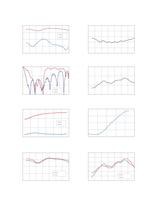
20100-10-2068101214161820FREQUENCY (GHz) 54321068101214161820FREQUENCY (GHz) LSBUSB > CONV GAIN (dB) NOISE FIGURE (dB) 0-10-20-3001020304050FREQUENCY (GHz) 50-5-1068101214161820FREQUENCY (GHz) > IIP3 (dBm) RETURN LOSS (dB) RFLO > 20100-10-6-226101418LO POWER (dBm) 0-5-10-15 -20-505101520LO POWER (dBm) LSBUSB > IIP3 (dBm) CONV GAIN (dB) 2015105 068101214161820FREQUENCY (GHz) 20-2 -4-6-8-1068101214161820FREQUENCY (GHz) > IIP3 (dBm) CONV GAIN (dB) IF = 1 GHzIF = 2 GHz IF = 1 GHzIF = 2 GHz >
Open the catalog to page 3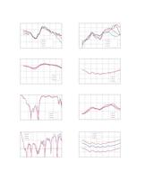
181614121068101214161820FREQUENCY (GHz) 20-2-4-6 -8-1068101214161820FREQUENCY (GHz) > CONV GAIN (dB) Vg = -1.2 VVg = -1.1 V Vg = -1.0 V Vg = -0.9 V > INPUT IP3 (dBm) Vg = -1.2 VVg = -1.1 V Vg = -1.0 V Vg = -0.9 V > 2015105068101214161820FREQUENCY (GHz) 54321068101214161820FREQUENCY (GHz) > CONV GAIN (dB) 4 V3 V 5 V > NOISE FIGURE (dB) 4 V3 V 5 V 0-10-20-3001020304050FREQUENCY (GHz) 50-5-1068101214161820FREQUENCY (GHz) > IIP3 (dBm) RETURN LOSS (dB) 25 n C-40 4 V3 V 5 V n C85 n C > 0-10-20-3001020304050FREQUENCY (GHz) 54321068101214161820FREQUENCY (GHz) 25 n C-40 25 n C-40 n C85 n C85 n C n C >...
Open the catalog to page 4
The AMMP Packaged Devices are compatible with high volume surface mount PCB assembly processes.The PCB material and mounting pattern, as defined in the data sheet, optimizes RF performance and is strong- ly recommended. An electronic drawing of the land pattern is available upon request from Agilent Sales & Application Engineering. > Figure 21. Suggested PCB Land Pattern and Stencil Layout Figure 23. Combined PCB and Stencil LayoutsFigure 22. Stencil Outline Drawing (mm) 7 >
Open the catalog to page 7All Avago Technologies catalogs and technical brochures
 AFCD-V84LP
1 Page
 BCM4778
2 Pages
 AFBR-57H5MZ
29 Pages
 ASMB-UTF0-0D20B
12 Pages
 ASMT-YTD7-0AA02
15 Pages
 ASMT-YTC7-0AA02
15 Pages
 ASMT-RF45-AN002
8 Pages
 Optical Sensor
64 Pages


Archived catalogs
 WLAN Low-Noise Amplifier
10 Pages
 Optoisolation Products
58 Pages
 125 Megabaud Versatile Link
12 Pages
 LED Solutions
96 Pages


- Display module
- Angular encoder
- Incremental encoder
- Incremental rotary encoder
- Switching relay
- Absolute rotary encoder
- Signal amplifying integrated circuit
- Transceiver module
- Optical rotary encoder
- Electronic filter
- Electronic display panel
- Magnetic rotary encoder
- Power amplifying integrated circuit
- Visible LED
- Diode
- Transistor module
- Solid state relay
- GNSS receiver
- Ethernet transceiver
- Data transceiver