
- Catalogs
- Avago Technologies
- 10GbE XFP 850 nm 10Gbps Optical Transceiver

10GbE XFP 850 nm 10Gbps Optical Transceiver

10GbE XFP 850 nm 10Gbps Optical Transceiver
Overview
The AFBR-720XPDZ is a 10GbE XFP optical transceiver module operating at 850 nm wavelength, designed for high-speed serial optical data communications at 9.9 to 10.325 Gb/s. It complies with IEEE 802.3ae 10GBASE-SR standards and RoHS directives, optimized for multimode fiber applications.
Key Features
- RoHS 6/6 compliant
- IEEE 802.3ae 10GBASE-SR compliance for 10 GbE at 10.325 Gb/s
- 3.3V single power supply operation
- 850 nm VCSEL laser and PIN photodiode from Avago Technologies
- No reference clock required
- LC duplex optical connector per ANSI/TIA/EIA-604-10 (FOCIS 10)
- Maximum power dissipation of 1.5 W
- Supports link lengths up to 300 m with OM3 fiber
- Operating case temperature range: 0 to +70 °C
- Superior thermal and EMI integrity for high port densities
- Customizable clip-on heatsink for various line card environments
- IEC 60825-1 Class 1 / CDRH Class 1 laser eye safety certified
Applications
- Fibre Channel switches
- Host bus adapter cards
- Mass storage systems and server I/O
- Ethernet switches
- Core routers
Description
The module integrates an 850 nm VCSEL laser transmitter with driver and signal conditioner ensuring low jitter and IEEE compliance. The receiver uses a PIN photodiode with low dark current and high responsivity. Digital diagnostics via a 2-wire serial interface provide real-time monitoring of temperature, supply voltage, laser bias current, output power, and received power. Features include transmitter disable, power down, fault monitoring, and receiver loss of signal detection.
Installation
Hot-pluggable into any compliant XFP port, allowing insertion during system operation. The housing design protects against ESD and ensures effective thermal contact with the heatsink through the cage.
Functional Description
Transmitter Section
Includes 850 nm VCSEL laser, driver, and signal conditioner. Optical output is controlled via a monitor photodiode and IC to maintain signal integrity over temperature and voltage variations. Transmitter can be disabled via pin 5 (TX_DIS) or serial interface.
Eye Safety Circuit
Laser power is maintained below Class 1 eye safety limits. In case of laser failure, the microcontroller and driver IC detect faults, shut down the laser, power down the module, and assert fault signals.
Receiver Section
Features PIN photodiode with amplification and signal conditioning. Includes Loss of Signal (RX_LOS) indicator to detect insufficient optical input power, signaling link failures. RX_LOS status accessible via serial interface.
Electrical Interface
Uses a 30-pin right-angle connector with 0.8 mm pitch. Provides internally AC-coupled, terminated differential data inputs and outputs, minimizing external components. Pinout includes power, ground, transmitter disable, receiver loss of signal, fault indicators, and two-wire serial interface (SDA, SCL).
Power Supply Filtering
Host board power supply filtering recommended with inductors and capacitors on +5 V, +3.3 V, +1.8 V, and -5.2 V lines to ensure stable operation.
Absolute Maximum Ratings
- Storage temperature: -40 to +85 °C
- Operating case temperature: 0 to +70 °C
- Supply voltage (VCC3): 0 to 3.6 V
- Power dissipation: max 1.5 W
- Relative humidity: 0 to 90%
Exceeding these limits may cause permanent damage.
Recommended Operating Conditions
- Supply voltage (VCC3): 3.135 to 3.465 V
- Data rate: 9.9 to 10.325 Gb/s
Electrical Characteristics
- Transmitter differential input impedance: 100 Ω ±5%
- Input differential amplitude: 120 to 820 mV peak-to-peak
- Receiver differential output amplitude: 340 to 850 mV peak-to-peak
- Jitter and eye mask compliant with IEEE 802.3ae
Optical Characteristics
- Laser output power: minimum -4.3 dBm typical
- Mean optical output power: -7.3 to -8 dBm
- Extinction ratio: minimum 3.0 dB
- Spectral width (rms): 0.45 nm typical
- Center wavelength: 840 to 860 nm
- Transmitter dispersion penalty: max 3.9 dB
- Receiver sensitivity: minimum -18.8 dBm
- Receiver reflectance: max -12 dB
Optical eye mask meets IEEE 802.3ae 10GBASE-SR requirements.
Timing Characteristics
- Transmitter disable assertion time: max 10 µs
- Transmitter disable negation time: max 2 ms
Timing and Signal Assertion Delays
- Initialization time after power-on or hot plug: 300 ms
- Interrupt assertion delay: 200 ms
- Interrupt negation delay: 500 µs
- Power-down/reset assertion: minimum 80 µs
- Power-down/reset negation: max 300 ms
- Fault indication assertion/negation: approx. 8 ms
- Module deselect assertion/de-assertion: max 2 ms
- Loss of signal (Rx_LOS) assertion: 800 µs
- Loss of signal negation: 2.3 ms
- Serial ID clock frequency: up to 400 kHz
Mechanical and Assembly Details
Module assembly includes clip, host board, heat sink, cage assembly, module bezel, EMI gasket, and connector. Temperature measurement points are defined on the module case. Mechanical drawings and host board layouts support integration.
Digital Diagnostic Interface and Serial Identification
Implements 2-wire serial interface compliant with XFP MSA Rev 4.0 and memory map Rev 2.0. The 256-byte I2C address space is divided into lower (128 bytes, always accessible for diagnostics) and upper blocks (serial ID, user EEPROM, reserved, vendor-specific). Diagnostics enable predictive failure identification, compliance prediction, fault isolation, and component monitoring.
Diagnostic Features and Monitoring Parameters
- Predictive Failure Identification: Early detection of potential link issues to enable failover and maintain uptime.
- Compliance Prediction: Real-time alerts when operating limits are exceeded, e.g., received optical power.
- Fault Isolation: Diagnostic data helps pinpoint link problems for faster servicing.
- Component Monitoring: Monitors internal temperature, laser bias current, transmitted and received optical power, and supply voltage.
Key Monitored Parameters
- Internal temperature on PCB (indicator of thermal drifts or failures)
- Laser DC bias current (closed-loop feedback for constant optical power)
- Transmitted average optical power (constant under normal operation)
- Received average optical power (for cable plant compliance and fault isolation)
- Auxiliary monitors including 3.3V supply voltage
Regulatory Compliance and Safety
- ESD Immunity: Tested per MIL-STD-883 Method 3015; withstands 500 V (high-speed pins), 2000 V (low-speed pins), 25 kV contact discharge on LC receptacle, 8 kV contact and 15 kV air discharge on optical connector.
- EMI Compliance: Meets FCC Class B, CENELEC EN55022 Class B, VCCI Class A; immunity testing shows no bit errors up to 80 V/m without chassis enclosure.
- Laser Safety: Certified Class 1 laser product under US FDA CDRH, IEC EN60825-1 and EN60825-2, with TUV certification.
- Flammability: Complies with UL 94V-0 standard.
Important: No user-serviceable parts inside. Tampering voids warranty and may cause failure or unsafe operation. Use only approved optical sources and operate within specified limits to avoid regulatory recertification.
Application Support and Ordering
Evaluation kits and reference designs are available to facilitate integration and testing. Customers should contact local sales representatives or authorized distributors for ordering. Additional technical resources and documentation are accessible via the manufacturer's website.
Catalog excerpts
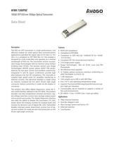
The 850 nm XFP transceiver is a high performance, cost eective module for serial optical data communications applications specied for signal rates of 9.9 Gb/s to 10.5 Gb/s. It is compliant to XFP MSA Rev 4.5. The module is designed for multi mode ber and operates at a nominal wavelength of 850 nm. The transmitter section incorpo- rates Avago Technologies 850 nm Vertical Cavity Surface Emitting Laser (VCSEL). The receiver section uses Avago TechnologiesҒ MOVPE grown planar SEDET PIN photo- detector for low dark current and excellent responsivity. Integrated Tx and Rx signal conditioners provide high jitter-tolerance for full XFI compliance. The internally ac coupled high speed serial I/O simplies interfacing to external circuitry. The electrical interface is made using an industry standard 0.8 mm pitch 30-pin right angle connector. Optical connection is made via the duplex LC connector.The product also oers digital diagnostics using the 2-wire serial interface dened in the XFP MSA. The product provides real time temperature (module and laser), sup- ply voltage, laser bias current, laser average output power and received input power. The digital diagnostic interface also adds the ability to disable the transmitter (TX_DIS), power down the module, monitor for module faults and monitor for Receiver Loss of Signal (RX_LOS). Transmitter disable, interrupt, power down/reset, receiver loss of sig- nal and module not ready are also hard wired pins on the 30-pin right angle connector. RoHS 6/6 Compliance Օ ComplianttoXFPMSACompliant to XFP MSA Compliant to IEEE 802.3ae 10GBASE-SR for 10GbE, 10.3125 Gb/s Օ Compliant XFI 10G Serial electrical interface 3.3V single power supply Օ Avago Technologies 850 nm VCSEL Laser and PIN Photodiode ҕ No reference clock required LC Duplex optical connector interface conforming to ANSI TIA/EIA604-10 (FOCIS 10) Օ 1.5W maximum Link Lengths up to 300 m with 0M3 ber Օ 0 to +70 C case operating temperature range Е Superior Thermal and EMI integrity performance to sup-port high port densities Customizable clip-on heatsink to support a variety of line card environments Օ IEC 60825-1 Class 1/CDRH Class 1 laser eye safety > Fiber Channel Switches Օ Host Bus Adapter Cards Mass Storage System and Server I/O Օ Ethernet Switches Core Routers 1 >
Open the catalog to page 1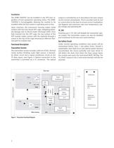
Heat sink Analog bus LaserRFdriver SignalConditioner +3.3V CWdriver Mon. PIN Digital 10Gb/s electricalI/O EEPROM > Analogsignalconditioners Microcontroller Digital lowspeed bus or signal > Optical receptacles Powersupplycontrol A/D > Electrical connector PIN TIA TIA Analog signal ROSA TOSA SignalConditioner Main housing ESA >
Open the catalog to page 2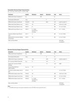
Dierential Input ImpedanceZ > d 100 ѢĦ Termination Mismatch ∆ Z > M 5%Dierential Input AmplitudeDVQDO120820mVpeak to peak (1) Dierential Input Return Loss SDD1120dB0.05 to 0.1 GHz Dierential Input Return Loss SDD118dB0.1 to 5.5 GHzDierential Input Return Loss SDD118 - 20.66 log10(f/5.5) f in GHz dB5.5 - 12 GHzCommon Mode Input Return LossSCC113dB0.1 to 15 GHzDierential to Common Mode ConversionSCD1110dB0.1 to 15 GHzJitter and Eye MaskXFP MSA Compliant > Dierential Input ImpedanceZ > d 100 Ω Termination Mismatch ∆ Z > M 5%Dierential Output Amplitude340850mVpeak to peak (1) DC Common Mode Potential...
Open the catalog to page 6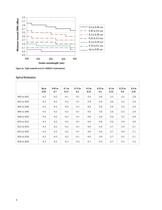
Center wavelength (nm) 0.4 to 0.45 nm0.35 to 0.4 nm 0.3 to 0.35 nm 0.25 to 0.3 nm 0.2 to 0.25 nm 0.15 to 0.2 nm Up to 0.05 nm -2.5-2.7-2.9-3.1-3.3-3.5-3.7-3.9-4.1-4.3-4.5840 > Minimum transmit OMA (dBm) 845850855860 > Figure 4a. Triple tradeo curve for 10GBASE-S (informative)
Open the catalog to page 8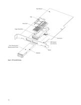
ClipHost Board Heat Sink Cage Assembly Case TemperatureMeasurement Point > ModuleBezelEMI Gasket(not shown)Connector > Figure 5. XFP Assembly Drawing 10 >
Open the catalog to page 10
The 2-wire serial interface is explicitly dened in the XFP MSA Rev 4.0. 2-wire timing specications and the struc- ture of the memory map are per XFP MSA Rev 2.0. The normal 256 Byte I2C address space is divided into lower and upper blocks of 128 Bytes. The lower block of 128 Bytes is always directly available and is used for diagnos- tic information providing the opportunity for Predictive Failure Identication, Compliance Prediction, Fault Isola- tion and Component Monitoring. The upper address space tables are used for less frequently accessed func- tions such as serial ID, user writeable EEPROM,...
Open the catalog to page 11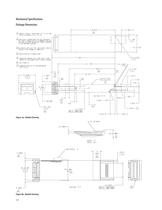
Figure 6a. Module Drawing Figure 6b. Module Drawing >
Open the catalog to page 12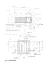
Figure 7. XFP host board mechanical layout 13 >
Open the catalog to page 13
An Evaluation Kit and Reference Designs are available to assist in evaluation of the AFBR-720XPDZ. Please con- tact your local Field Sales representative for availability and ordering details. There are two conditions in which immunity to ESD damage is important. Table 13 documents the ESD im- munity to both of these conditions.The rst condition is static discharge to the transceiver during handling such as when the transceiver is inserted into the transceiver port. To protect the transceiver, it is important to use normal ESD handling precautions in- cluding the use of grounded wrist straps,...
Open the catalog to page 14
The transceivers have a shielded design to provide excel-lent immunity to radio-frequency electromagnetic elds which may be present in some operating environments. The AFBR-720XPDZ contains no user serviceable parts. Tampering with or modifying the performance of the AFBR-720XPDZ will result in voided product warranty. It may also result in improper operation of the AFBR- 720XPDZ circuitry, and possible overstress of the laser source. Device degradation or product failure may result. Connection of the AFBR-720XPDZ to a non-approved op- tical source, operating above the recommended absolute maximum...
Open the catalog to page 15All Avago Technologies catalogs and technical brochures
 AFCD-V84LP
1 Page
 BCM4778
2 Pages
 AFBR-57H5MZ
29 Pages
 ASMB-UTF0-0D20B
12 Pages
 ASMT-YTD7-0AA02
15 Pages
 ASMT-YTC7-0AA02
15 Pages
 ASMT-RF45-AN002
8 Pages
 Optical Sensor
64 Pages


Archived catalogs
 WLAN Low-Noise Amplifier
10 Pages
 Optoisolation Products
58 Pages
 125 Megabaud Versatile Link
12 Pages
 LED Solutions
96 Pages


- Display module
- Angular encoder
- Incremental encoder
- Incremental rotary encoder
- Switching relay
- Absolute rotary encoder
- Signal amplifying integrated circuit
- Electronic display panel
- Optical rotary encoder
- Electronic filter
- Magnetic rotary encoder
- Power amplifying integrated circuit
- Diode
- Visible LED
- Transistor module
- Solid state relay
- GNSS receiver
- Ethernet transceiver
- Rectifier diode