ATtiny24/44/84 Automotive Preliminary
1 /225Pages

ATtiny24/44/84 Automotive Preliminary
1 /225Pages
Catalog excerpts

High Performance, Low Power AVR > ծ 8-Bit Microcontroller > Advanced RISC ArchitectureՖ120 Powerful Instructions Most Single Clock Cycle Execution֖32 x 8 General Purpose Working RegistersFully Static Operation > Non-volatile Program and Data Memories2/4/8K Byte of In-System Programmable Program Memory Flash (ATtiny24/44/84)Endurance: 10,000 Write/Erase Cycles֖128/256/512 Bytes In-System Programmable EEPROM (ATtiny24/44/84)Endurance: 100,000 Write/Erase Cycles128/256/512 Bytes Internal SRAM (ATtiny24/44/84) ֖Programming Lock for Self-Programming Flash Program and EEPROM Data Security > Peripheral FeaturesՖTwo Timer/Counters, 8- and 16-bit counters with two PWM Channels on both10-bit ADC8 single-ended channels 12 differential ADC channel pairs with programmable gain (1x, 20x)Temperature Measurement֖Programmable Watchdog Timer with Separate On-chip Oscillator On-chip Analog Comparator֖Universal Serial Interface > Special Microcontroller FeaturesՖdebugWIRE On-chip Debug SystemIn-System Programmable via SPI Port֖External and Internal Interrupt Sources Pin Change Interrupt on 12 pins֖Low Power Idle, ADC Noise Reduction, Standby and Power-down ModesEnhanced Power-on Reset Circuit ֖Programmable Brown-out Detection CircuitInternal Calibrated Oscillator֖On-chip Temperature Sensor > I/O and PackagesՖ14-pin SOIC, 20-pin QFN/MLF: Twelve Programmable I/O Lines > Automotive Temperature Range > Low Power ConsumptionActive Mode: 1 MHz, 2.7V: 800 ֵAPower-down Mode: 2.7V: 2.0 ֵA > Rev. 7701BAVR֖09/07 size="-1">
Open the catalog to page 1
2.3.1VCC Supply voltage. 2.3.2GND Ground. 2.3.3Port B (PB3...PB0) Port B is a 4-bit bi-directional I/O port with internal pull-up resistors (selected for each bit). The Port B output buffers have symmetrical drive characteristics with both high sink and source capability except PB3 which has the RESET capability. To use pin PB3 as an I/O pin, instead of RESET pin, program (0ђ) RSTDISBL fuse. As inputs, Port B pins that are externally pulled low will source current if the pull-up resistors are activated. The Port B pins are tri-stated when a reset condition becomes active, even if the clock is...
Open the catalog to page 5
A comprehensive set of development tools, drivers and application notes, and datasheets are available for download on http://www.atmel.com/avr. > This documentation contains simple code examples that briefly show how to use various parts of the device. These code examples assume that the part specific header file is included before compilation. Be aware that not all C compiler vendors include bit definitions in the header files and interrupt handling in C is compiler dependent. Please confirm with the C compiler documen-tation for more details.For I/O Registers located in extended I/O map, INӔ,...
Open the catalog to page 6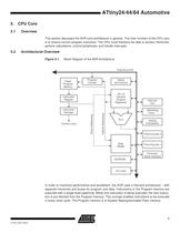
Data Bus 8-bit > Flash ProgramCounter Statusand Control I/O LinesEEPROM ProgramMemory 32 x 8GeneralPurposeRegistrers > InterruptUnit InstructionDecoder WatchdogTimerAnalogComparator ALU Control Lines > Direct AddressingIndirect Addressing Timer/Counter 0 DataSRAM Timer/Counter 1Universal Serial Interface >
Open the catalog to page 7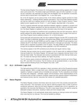
The fast-access Register File contains 32 x 8-bit general purpose working registers with a single clock cycle access time. This allows single-cycle Arithmetic Logic Unit (ALU) operation. In a typ-ical ALU operation, two operands are output from the Register File, the operation is executed, and the result is stored back in the Register File in one clock cycle.Six of the 32 registers can be used as three 16-bit indirect address register pointers for Data Space addressing ֖ enabling efficient address calculations. One of the these address pointers can also be used as an address pointer for look...
Open the catalog to page 8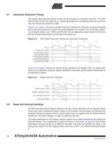
This section describes the general access timing concepts for instruction execution. The AVR CPU is driven by the CPU clock clk > CPU , directly generated from the selected clock source for the chip. No internal clock division is used.Figure 5-4 on page 12 shows the parallel instruction fetches and instruction executions enabled by the Harvard architecture and the fast access Register File concept. This is the basic pipelin- ing concept to obtain up to 1 MIPS per MHz with the corresponding unique results for functions per cost, functions per clocks, and functions per power-unit. Figure 5-4. The...
Open the catalog to page 12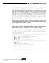
in r16, SREG ; store SREG value cli ; disable interrupts during timed sequence sbi EECR, EEMPE ; start EEPROM write sbi EECR, EEPE out SREG, r16 ; restore SREG value (I-bit) > char cSREG;cSREG = SREG; /* store SREG value */ /* disable interrupts during timed sequence */ _CLI(); EECR |= (1<SREG = cSREG; >
Open the catalog to page 13
sei ; set Global Interrupt Enable sleep ; enter sleep, waiting for interrupt ; note: will enter sleep before any pending ; interrupt(s) > _SEI(); /* set Global Interrupt Enable */ _SLEEP(); /* enter sleep, waiting for interrupt */ /* note: will enter sleep before any pending interrupt(s) */ >
Open the catalog to page 14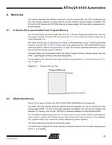
This section describes the different memories in the ATtiny24/44/84. The AVR architecture has two main memory spaces, the Data memory and the Program memory space. In addition, the ATtiny24/44/84 features an EEPROM Memory for data storage. All three memory spaces are lin-ear and regular. > The ATtiny24/44/84 contains 2/4/8K byte On-chip In-System Reprogrammable Flash memory for program storage. Since all AVR instructions are 16 or 32 bits wide, the Flash is organized as 1024/2048/4096 x 16.The Flash memory has an endurance of at least 10,000 write/erase cycles. The ATtiny24/44/84Program Counter...
Open the catalog to page 15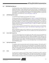
The ATtiny24/44/84 contains 128/256/512 bytes of data EEPROM memory. It is organized as a separate data space, in which single bytes can be read and written. The EEPROM has an endurance of at least 100,000 write/erase cycles. The access between the EEPROM and the CPU is described in the following, specifying the EEPROM Address Registers, the EEPROM Data Register, and the EEPROM Control Register. For a detailed description of Serial data downloading to the EEPROM, see Serial DownloadingԔ on page 168. 6.3.1EEPROM Read/Write Access The EEPROM Access Registers are accessible in the I/O space.The...
Open the catalog to page 17All Atmel catalogs and technical brochures
 32-bit Microcontrollers
20 Pages
 MCUs Driving Displays
12 Pages
 Touch and 3D Gesture Control
12 Pages
 16-bit MCUs and DSCs
20 Pages
 XLP PIC® MCUs
8 Pages
 8-bit MCUs
16 Pages
 AT93C56B/66B Automotive
17 Pages
 Atmel AT86RF215 Device Family
235 Pages
 AT24C01C/02C
22 Pages
 maXTouch U Series - Flyer
2 Pages


Archived catalogs
 tinyAVR ATtiny24/44/84 Preliminary
240 Pages
 ATmega164P/324P/644P Preliminary
440 Pages
 ATmega48P/88P/168P/328P Preliminary
426 Pages
 ATmega1284P Preliminary
356 Pages
 AT90PWM216/316
359 Pages
 AT90PWM2, AT90PWM3, AT90PWM2B, AT90PWM3B
361 Pages
 ATmega329/3290/649/6490 Preliminary
392 Pages
 ATmega329P/3290P Preliminary
388 Pages
 AT90CAN32/64/128
428 Pages
 AT86RF230 Preliminary
98 Pages
 ATmega48/88/168 Automotive
335 Pages
 ATtiny25, ATtiny45, ATtiny85 Automotive
192 Pages
 AT86RF231 Preliminary
180 Pages
 Biometrics (Fingerprint Sensor)
20 Pages


- Transceiver module
- Potentiometer
- Industrial converter
- Ethernet transceiver
- Analog potentiometer
- Low-noise amplifier
- Analog amplifier
- Analog converter
- Circuit board
- Operational amplifier
- 32-bit microcontroller
- Low-power microcontroller
- Analog microcontroller
- High-speed converter
- General purpose microcontroller
- DAC converter
- Communication microcontroller
- High-speed amplifier
- ARM microcontroller