Atmel AT86RF215 Device Family
1 /235Pages

Atmel AT86RF215 Device Family
1 /235Pages
Catalog excerpts

Atmel AT86RF215 Device Family Sub-1GHz/2.4GHz Transceiver and I/Q Radio for Features AT86RF215 • Fully integrated radio transceiver covering 389.5-510MHz / 779-1020MHz / 2400-2483.5MHz including: • European band: • Chinese band: • North American band: • Korean band: • Japanese band: • I/Q data interface: • One TX and two RX serial low voltage differential signal (LVDS) interfaces • 13-bit I/Q data interface with a sampling frequency of up to 4MHz • Transceiver Control interface: SPI (serial peripheral interface) • Supported PHYs (*proprietary) • MR-FSK • Symbol rates: 50, 100, 150, 200, 300*, 400ksymbol/s • Rate 1/2-FEC: RSC and NRNSC, with and without interleaving • Order: 2-level, 4-level • MR-OFDM • Option 1: 100, 200, 400, 800, 1200*, 1600*, 2400*kb/s • Option 2: 50, 100, 200, 400, 600, 800, 1200*kb/s • Option 3: 50, 100, 200, 300, 400, 600kb/s • Option 4: 50, 100, 150, 200, 300kb/s • MR-O-QPSK • 100kchip/s with 6.25, 12.5, 25, 50kb/s data rate • 200kchip/s with 12.5, 25*, 50*, 100*kb/s data rate • 1000kchip/s with 31.25, 125, 250, 500kb/s data rate • 2000kchip/s with 31.25, 125, 250, 500, 1000*kb/s data rate • O-QPSK • 1000kchip/s with 250kb/s and 500*kb/s data rate • 2000kchip/s with 250kb/s and 1000*kb/s data rate • Bi-directional differential RF signal ports for: • Band I: 433/470/780/863/868/915/917/920MHz • Band II: 2450MHz
Open the catalog to page 1
• Simultaneous operation of sub-1GHz and 2.4GHz transceiver • Separate 2kbytes RX and TX frame buffer • IEEE MAC support • Frame filter (IEEE Std 802.15.4-2006) • FCS handling • Automatic acknowledgement (IEEE Std 802.15.4-2006) • CCA with automatic transmit • Industry leading link budget • Programmable TX output power up to +14.5dBm@900MHz band • Noise figure below 5dB for sub-1GHz and 2.4GHz transceiver • Receiver sensitivity down to -123dBm at 6.25kb/s MR-O-QPSK • Radio transceiver features • Integrated TX/RX switch, LNA, PLL loop filter and RF frontend control • Fast settling PLL supporting...
Open the catalog to page 2
1. Description The AT86RF215 is a multi-band radio transceiver for various sub-1GHz bands and the 2.4GHz band specially designed for smart metering and applications implementing IEEE Std 802.15.4g™-2012 [3], ETSI TS 102 887-1 [5], IEEE Std 802.15.4TM-2015 [7]. The device is comprised of two independent transceivers, each with its own baseband and I/Q data interface. The AT86RF215 incorporates two transceivers and two baseband cores forming two independent radio systems. The transceivers are highly integrated minimizing the number of external components required on the printed circuit board (PCB)....
Open the catalog to page 3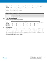
Read/Write RRRRRRRR • Bit 7:0 - RF_PN.PN: Device Part Number The register contains the part number of the device. 1.1.3.2 RF_VN - Device Version Number The register contains the version number of the device. Bit 7 6 5 4 3 2 1 0 Read/Write RRRRRRRR 1.2 Block Diagram The device features two independent radio systems. It contains one sub-1GHz transceiver and one 2.4GHz transceiver. Each transceiver is paired with a baseband core optimized to demodulate signals commonly used in the associated band, thus providing complete RF-to-Baseband operation. The internal baseband...
Open the catalog to page 4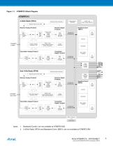
Figure 1-1. AT86RF215 Block Diagram Random Number Generator Battery Monitor (BATMON) DVDD (1.8V) Digital Voltage Regulator Automatic Gain Control (AGC) Receiver Analog Frontend Receiver Digital Frontend Sigma-Delta Analog Digital Converter (SDADC) Band Pass Filter (BPF) Filter, DownSampling (RX_DFE) Baseband Core1 (BBC1) RX Frame Buffer AVDD1 (1.8V) Analog Voltage Regulator (2.4GHz Transceiver) Transmitter Analog Frontend Analog Calibration MR-OFDM Transmitter Digital Frontend Low Pass Filter (LPF) Digital Analog Converter (DAC) Filter, UpSampling (TX_DFE) MR-O-QPSK/ O-QPSK TX Frame Buffer Serial...
Open the catalog to page 5
Control Logic and Naming Conventions Both radio and baseband cores have separate register blocks. The sub-1GHz radio register names are prefixed by “RF09_”. The 2.4GHz radio transceiver register names are prefixed by “RF24_”. The register descriptions, including sub-register descriptions, for both radios and their respective basebands are identical. In rare cases where a register is only valid for one specific radio (or baseband), the register for the other radio (or baseband) is ignored. The baseband processor Core0 is connected to the sub-1GHz radio and Core1 is connected to the 2.4GHz radio....
Open the catalog to page 6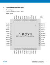
Pin-out Diagram and Description Pin-out Diagram The pin-out of the AT86RF215 is shown in Figure 2-1. PADDLE (AVSS)
Open the catalog to page 7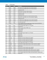
yitmel Atmel AT86RF215 - DATASHEET 8 Atmel-42415E-WIRELESS-RF215_Datasheet_052016
Open the catalog to page 8
2.2.1 RFP09/RFN09, RFP24/RFN24 The differential RF pins (RFP09/RFN09; RFP24/RFN24) provide common-mode rejection to suppress the switching noise of the internal and external digital signal processing blocks. A 500 differential load at the RF ports ensures high sensitivity and output power. A DC path between the RF pins is supported; a DC path to ground or supply voltage is not supported. When connecting an RF load providing a DC path to the power supply or ground, AC coupling is required. The pins RFP24/RFN24 of AT86RF215M are shortened to AVSS internally and may not be connected. 2.2.2 EVDD,...
Open the catalog to page 9
MISO, MOSI, SCLK, SELN Pins MISO, MOSI, SCLK and SELN are SPI specific pins which provide register read/write access for device operation. For further information about the control interface see section "SPI Transceiver Control Interface" on page 16. RXDN09/RXDP09, RXDN24/RXDP24, RXCLKP/RXCLKN, TXDP/TXDN, TXCLKP/TXCLKN Pins RXDN09/RXDP09, RXDN24/RXDP24, RXCLKP/RXCLKN, TXDP/TXDN and TXCLKP/TXCLKN are low voltage differential signal (LVDS) I/Q data interface pins. For further information see section "Serial I/Q Data Interface" on page 22. The pins RXDN24/RXDP24 are not supported for AT86RF215M,...
Open the catalog to page 10All Atmel catalogs and technical brochures
 32-bit Microcontrollers
20 Pages
 MCUs Driving Displays
12 Pages
 Touch and 3D Gesture Control
12 Pages
 16-bit MCUs and DSCs
20 Pages
 XLP PIC® MCUs
8 Pages
 8-bit MCUs
16 Pages
 AT93C56B/66B Automotive
17 Pages
 AT24C01C/02C
22 Pages
 maXTouch U Series - Flyer
2 Pages


Archived catalogs
 tinyAVR ATtiny24/44/84 Preliminary
240 Pages
 ATmega164P/324P/644P Preliminary
440 Pages
 ATmega48P/88P/168P/328P Preliminary
426 Pages
 ATmega1284P Preliminary
356 Pages
 AT90PWM216/316
359 Pages
 AT90PWM2, AT90PWM3, AT90PWM2B, AT90PWM3B
361 Pages
 ATmega329/3290/649/6490 Preliminary
392 Pages
 ATmega329P/3290P Preliminary
388 Pages
 AT90CAN32/64/128
428 Pages
 AT86RF230 Preliminary
98 Pages
 ATmega48/88/168 Automotive
335 Pages
 ATtiny25, ATtiny45, ATtiny85 Automotive
192 Pages
 ATtiny24/44/84 Automotive Preliminary
225 Pages
 AT86RF231 Preliminary
180 Pages
 Biometrics (Fingerprint Sensor)
20 Pages


- Potentiometer
- Industrial converter
- Ethernet transceiver
- Analog potentiometer
- Low-noise amplifier
- Microcontroller
- Analog amplifier
- Operational amplifier
- 32-bit microcontroller
- Low-power microcontroller
- Analog microcontroller
- High-speed converter
- General purpose microcontroller
- DAC converter
- Communication microcontroller
- High-speed amplifier
- ARM microcontroller