ATmega640/1280/1281/2560/2561 Preliminary
1 /448Pages

ATmega640/1280/1281/2560/2561 Preliminary
1 /448Pages
Catalog excerpts

Typical values contained in this datasheet are based on simulations and characterization ofother AVR microcontrollers manufactured on the same process technology. Min. and Max val-ues will be available after the device is characterized. 4 >
Open the catalog to page 4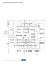
PF7..0 PK7..0 PJ7..0 PE7..0 > PowerSupervisionPOR / BOD &RESET RESET PORT F (8) PORT K (8) PORT J (8) PORT E (8) > W atchdogTimer G N D VCC W atchdogOscillator JTAG A/DConverter USART 0 > XTAL1XTAL2 OscillatorCircuits /ClockGeneration EEPROM Internal Bandgap referenceAnalog Comparator 16bit T/C 3 16bit T/C 5 USART 3 > CPU PA7..0 PORT A (8) 16bit T/C 4 USART 1 PG5..0 PORT G (6) XRAM FLASH SRAM 16bit T/C 1 PC7..0 PORT C (8) T W I SPI 8bit T/C 0 8bit T/C 2 USART 2 > PORT D (8) PORT B (8) PORT H (8) PORT L (8) PD7..0 PB7..0 PH7..0 PL7..0 >
Open the catalog to page 5
The AVR core combines a rich instruction set with 32 general purpose working registers. All the32 registers are directly connected to the Arithmetic Logic Unit (ALU), allowing two independentregisters to be accessed in one single instruction executed in one clock cycle. The resultingarchitecture is more code efficient while achieving throughputs up to ten times faster than con-ventional CISC microcontrollers.The ATmega640/1280/1281/2560/2561 provides the following features: 64K/128K/256K bytes ofIn-System Programmable Flash with Read- W hile- W rite capabilities, 4K bytes EEPROM, 8Kbytes SRAM,...
Open the catalog to page 6
resistors are activated. The Port H pins are tri-stated when a reset condition becomes active,even if the clock is not running.Port H also serves the functions of various special features of the ATmega640/1280/2560 aslisted on page 92. 3.3.11Port J (PJ7..PJ0) Port J is a 8-bit bi-directional I/O port with internal pull-up resistors (selected for each bit). ThePort J output buffers have symmetrical drive characteristics with both high sink and source capa-bility. As inputs, Port J pins that are externally pulled low will source current if the pull-upresistors are activated. The Port J pins are...
Open the catalog to page 9
3.3.17AVCC AVCC is the supply voltage pin for Port F and the A/D Converter. It should be externally con-nected to V > CC , even if the ADC is not used. If the ADC is used, it should be connected to V > CC through a low-pass filter. 3.3.18AREF This is the analog reference pin for the A/D Converter. > A comprehensive set of development tools and application notes, and datasheets are availablefor download on http://www.atmel.com/avr. > This documentation contains simple code examples that briefly show how to use various parts ofthe device. Be aware that not all C compiler vendors include bit definitions...
Open the catalog to page 10
The Status Register contains information about the result of the most recently executed arith-metic instruction. This information can be used for altering program flow in order to performconditional operations. N ote that the Status Register is updated after all ALU operations, asspecified in the Instruction Set Reference. This will in many cases remove the need for using thededicated compare instructions, resulting in faster and more compact code.The Status Register is not automatically stored when entering an interrupt routine and restoredwhen returning from an interrupt. This must be handled...
Open the catalog to page 13
Figure 7-6. The Parallel Instruction Fetches and Instruction Executions Figure 7-7 shows the internal timing concept for the Register File. In a single clock cycle an ALUoperation using two register operands is executed, and the result is stored back to the destina- tion register. > T1T2T3T4 clk1st Instruction Fetch1st Instruction Execute2nd Instruction Fetch2nd Instruction Execute3rd Instruction Fetch3rd Instruction Execute4th Instruction Fetch CPU Figure 7-7. Single Cycle ALU Operation > T1T2T3T4 clk CPU Total Execution TimeRegister Operands FetchALU Operation ExecuteResult Write Back The AVR...
Open the catalog to page 17
in r16, SREG ; store SREG value cli ; disable interrupts during timed sequence sbi EECR, EEMPE ; start EEPROM write sbi EECR, EEPE out SREG, r16 ; restore SREG value (I-bit) > char cSREG;cSREG = SREG; /* store SREG value */ /* disable interrupts during timed sequence */ __disable_interrupt(); EECR |= (1<
Open the catalog to page 18
sei ; set Global Interrupt Enable sleep ; enter sleep, waiting for interrupt ; note: will enter sleep before any pending ; interrupt(s) > __enable_interrupt(); /* set Global Interrupt Enable */ __sleep(); /* enter sleep, waiting for interrupt */ /* note: will enter sleep before any pending interrupt(s) */ >
Open the catalog to page 19
file, the next 64 location the standard I/O Memory, then 416 locations of Extended I/O memoryand the next 8,192 locations address the internal data SRAM.An optional external data SRAM can be used with the ATmega640/1280/1281/2560/2561. ThisSRAM will occupy an area in the remaining address locations in the 64K address space. Thisarea starts at the address following the internal SRAM. The Register file, I/O, Extended I/O andInternal SRAM occupies the lowest 4,608/8,704 bytes, so when using 64KB (65,536 bytes) ofExternal Memory, 60,478/56,832 Bytes of External Memory are available. See External...
Open the catalog to page 21
Figure 8-2. Data Memory Map > Address (HEX) 0 - 1F32 Registers20 - 5F64 I/O Registers60 - 1FF 416 External I/O Registers200 Internal SRAM(8192 x 8)21FF2200 External SRAM(0 - 64K x 8)FFFF 8.2.1Data Memory Access Times This section describes the general access timing concepts for internal memory access. Theinternal data SRAM access is performed in two clk > CPU cycles as described in Figure 8-3. Figure 8-3. On-chip Data SRAM Access Cycles > CPU Address validT1T2T3Compute Address ReadWrite Memory Access InstructionNext Instruction The ATmega640/1280/1281/2560/2561 contains 4K bytes of data EEPROM...
Open the catalog to page 22
8.3.1EEPROM Read/Write Access The EEPROM Access Registers are accessible in the I/O space, see Register DescriptionӔ onpage 34.The write access time for the EEPROM is given in Table 8-4 on page 23. A self-timing function,however, lets the user software detect when the next byte can be written. If the user code con-tains instructions that write the EEPROM, some precautions must be taken. In heavily filtered power supplies, V > CC is likely to rise or fall slowly on power-up/down. This causes the device forsome period of time to run at a voltage lower than specified as minimum for the clock frequencyused....
Open the catalog to page 23All Atmel catalogs and technical brochures
 32-bit Microcontrollers
20 Pages
 MCUs Driving Displays
12 Pages
 Touch and 3D Gesture Control
12 Pages
 16-bit MCUs and DSCs
20 Pages
 XLP PIC® MCUs
8 Pages
 8-bit MCUs
16 Pages
 AT93C56B/66B Automotive
17 Pages
 Atmel AT86RF215 Device Family
235 Pages
 AT24C01C/02C
22 Pages
 maXTouch U Series - Flyer
2 Pages


Archived catalogs
 tinyAVR ATtiny24/44/84 Preliminary
240 Pages
 ATmega164P/324P/644P Preliminary
440 Pages
 ATmega48P/88P/168P/328P Preliminary
426 Pages
 ATmega1284P Preliminary
356 Pages
 AT90PWM216/316
359 Pages
 AT90PWM2, AT90PWM3, AT90PWM2B, AT90PWM3B
361 Pages
 ATmega329/3290/649/6490 Preliminary
392 Pages
 ATmega329P/3290P Preliminary
388 Pages
 AT90CAN32/64/128
428 Pages
 AT86RF230 Preliminary
98 Pages
 ATmega48/88/168 Automotive
335 Pages
 ATtiny25, ATtiny45, ATtiny85 Automotive
192 Pages
 ATtiny24/44/84 Automotive Preliminary
225 Pages
 AT86RF231 Preliminary
180 Pages
 Biometrics (Fingerprint Sensor)
20 Pages


- Transceiver module
- Potentiometer
- Industrial converter
- Ethernet transceiver
- Analog potentiometer
- Low-noise amplifier
- Analog amplifier
- Analog converter
- Circuit board
- Operational amplifier
- 32-bit microcontroller
- Low-power microcontroller
- Analog microcontroller
- High-speed converter
- General purpose microcontroller
- DAC converter
- Communication microcontroller
- High-speed amplifier
- ARM microcontroller