ATmega48P/88P/168P/328P Preliminary
1 /426Pages

ATmega48P/88P/168P/328P Preliminary
1 /426Pages
Catalog excerpts
1.1.1VCC Digital supply voltage. 1.1.2GND Ground. 1.1.3Port B (PB7:0) XTAL1/XTAL2/TOSC1/TOSC2 Port B is an 8-bit bi-directional I/O port with internal pull-up resistors (selected for each bit). ThePort B output buffers have symmetrical drive characteristics with both high sink and sourcecapability. As inputs, Port B pins that are externally pulled low will source current if the pull-up resistors are activated. The Port B pins are tri-stated when a reset condition becomes active,even if the clock is not running.Depending on the clock selection fuse settings, PB6 can be used as input to the inverting...
Open the catalog to page 3
The various special features of Port D are elaborated in Alternate Functions of Port DԔ on page89. 1.1.7AV > CC AV > CC is the supply voltage pin for the A/D Converter, PC3:0, and ADC7:6. It should be externallyconnected to V > CC , even if the ADC is not used. If the ADC is used, it should be connected to V > CC through a low-pass filter. Note that PC6..4 use digital supply voltage, V > CC . 1.1.8AREF AREF is the analog reference pin for the A/D Converter. 1.1.9ADC7:6 (TQFP and QFN/MLF Package Only) In the TQFP and QFN/MLF package, ADC7:6 serve as analog inputs to the A/D converter.These pins...
Open the catalog to page 4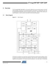
VCCGND WatchdogTimer PowerSupervisionPOR / BOD &RESET debugWIRE WatchdogOscillator > PROGRAMLOGIC OscillatorCircuits /ClockGeneration Flash SRAM CPU EEPROM > GNDAREFAVCC 8bit T/C 0 16bit T/C 1 A/D Conv. > 2 8bit T/C 2 AnalogComp. InternalBandgap > 6 DATABUS USART 0 SPI TWI PORT D (8) PORT B (8) PORT C (7) > RESET XTAL[1..2] ADC[6..7]PC[0..6]PB[0..7]PD[0..7]
Open the catalog to page 5
architecture is more code efficient while achieving throughputs up to ten times faster than con-ventional CISC microcontrollers.The ATmega48P/88P/168P/328P provides the following features: 4K/8K/16K/32K bytes of In-System Programmable Flash with Read-While-Write capabilities, 256/512/512/1K bytesEEPROM, 512/1K/1K/2K bytes SRAM, 23general purpose I/O lines, 32 general purpose work-ing registers, three flexible Timer/Counters with compare modes, internal and externalinterrupts, a serial programmable USART, a byte-oriented 2-wire Serial Interface, an SPI serialport, a 6-channel 10-bit ADC (8 channels...
Open the catalog to page 6
A comprehensive set of development tools, application notes and datasheets are available fordownload on http://www.atmel.com/avr. 7 > 8025DAVR֖03/08 size="-1">
Open the catalog to page 7
Reliability Qualification results show that the projected data retention failure rate is much lessthan 1 PPM over 20 years at 85C or 100 years at 25аC. > This documentation contains simple code examples that briefly show how to use various parts ofthe device. These code examples assume that the part specific header file is included before compilation. Be aware that not all C compiler vendors include bit definitions in the header filesand interrupt handling in C is compiler dependent. Please confirm with the C compiler documen-tation for more details.For I/O Registers located in extended I/O map,...
Open the catalog to page 8
ical ALU operation, two operands are output from the Register File, the operation is executed,and the result is stored back in the Register File in one clock cycle.Six of the 32 registers can be used as three 16-bit indirect address register pointers for DataSpace addressing ֖ enabling efficient address calculations. One of the these address pointerscan also be used as an address pointer for look up tables in Flash program memory. Theseadded function registers are the 16-bit X-, Y-, and Z-register, described later in this section.The ALU supports arithmetic and logic operations between registers...
Open the catalog to page 10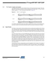
6.4.1The X-register, Y-register, and Z-register The registers R26..R31 have some added functions to their general purpose usage. These reg-isters are 16-bit address pointers for indirect addressing of the data space. The three indirectaddress registers X, Y, and Z are defined as described in Figure 6-3. Figure 6-3. The X-, Y-, and Z-registers In the different addressing modes these address registers have functions as fixed displacement,automatic increment, and automatic decrement (see the instruction set reference for details). > 15XHXL0X-register7070R27 (0x1B)R26 (0x1A)15YHYL0Y-register7070R29...
Open the catalog to page 13
The AVR provides several different interrupt sources. These interrupts and the separate ResetVector each have a separate program vector in the program memory space. All interrupts areassigned individual enable bits which must be written logic one together with the Global InterruptEnable bit in the Status Register in order to enable the interrupt. Depending on the ProgramCounter value, interrupts may be automatically disabled when Boot Lock bits BLB02 or BLB12are programmed. This feature improves software security. See the section Memory Program-mingԔ on page 294 for details.The lowest addresses...
Open the catalog to page 15
in r16, SREG ; store SREG value cli ; disable interrupts during timed sequence sbi EECR, EEMPE ; start EEPROM write sbi EECR, EEPE out SREG, r16 ; restore SREG value (I-bit) > char cSREG;cSREG = SREG; /* store SREG value */ /* disable interrupts during timed sequence */ _CLI(); EECR |= (1< sei ; set Global Interrupt Enable sleep ; enter sleep, waiting for interrupt ; note: will enter sleep before any pending interrupt(s) > __enable_interrupt(); /* set Global Interrupt Enable */ __sleep(); /* enter sleep, waiting for interrupt */ /* note: will enter sleep before any pending interrupt(s) */ >
Open the catalog to page 16
This section describes the different memories in the ATmega48P/88P/168P/328P. The AVRarchitecture has two main memory spaces, the Data Memory and the Program Memory space. In addition, the ATmega48P/88P/168P/328P features an EEPROM Memory for data storage. Allthree memory spaces are linear and regular. > The ATmega48P/88P/168P/328P contains 4/8/16/32K bytes On-chip In-System Reprogramma-ble Flash memory for program storage. Since all AVR instructions are 16 or 32 bits wide, theFlash is organized as 2/4/8/16K x 16. For software security, the Flash Program memory space isdivided into two sections,...
Open the catalog to page 17All Atmel catalogs and technical brochures
 32-bit Microcontrollers
20 Pages
 MCUs Driving Displays
12 Pages
 Touch and 3D Gesture Control
12 Pages
 16-bit MCUs and DSCs
20 Pages
 XLP PIC® MCUs
8 Pages
 8-bit MCUs
16 Pages
 AT93C56B/66B Automotive
17 Pages
 Atmel AT86RF215 Device Family
235 Pages
 AT24C01C/02C
22 Pages
 maXTouch U Series - Flyer
2 Pages


Archived catalogs
 tinyAVR ATtiny24/44/84 Preliminary
240 Pages
 ATmega164P/324P/644P Preliminary
440 Pages
 ATmega1284P Preliminary
356 Pages
 AT90PWM216/316
359 Pages
 AT90PWM2, AT90PWM3, AT90PWM2B, AT90PWM3B
361 Pages
 ATmega329/3290/649/6490 Preliminary
392 Pages
 ATmega329P/3290P Preliminary
388 Pages
 AT90CAN32/64/128
428 Pages
 AT86RF230 Preliminary
98 Pages
 ATmega48/88/168 Automotive
335 Pages
 ATtiny25, ATtiny45, ATtiny85 Automotive
192 Pages
 ATtiny24/44/84 Automotive Preliminary
225 Pages
 AT86RF231 Preliminary
180 Pages
 Biometrics (Fingerprint Sensor)
20 Pages


- Transceiver module
- Potentiometer
- Industrial converter
- Ethernet transceiver
- Analog potentiometer
- Low-noise amplifier
- Analog amplifier
- Analog converter
- Circuit board
- Operational amplifier
- 32-bit microcontroller
- Low-power microcontroller
- Analog microcontroller
- High-speed converter
- General purpose microcontroller
- DAC converter
- Communication microcontroller
- High-speed amplifier
- ARM microcontroller