ATmega48/88/168 Automotive
1 /335Pages

ATmega48/88/168 Automotive
1 /335Pages
Catalog excerpts

High Performance, Low Power AVR > ծ 8-Bit Microcontroller > Advanced RISC ArchitectureՖ131 Powerful Instructions Most Single Clock Cycle Execution֖32 x 8 General Purpose Working RegistersFully Static Operation ֖Up to 16 MIPS Throughput at 16 MHzOn-chip 2-cycle Multiplier > Non-volatile Program and Data Memories4/8/16K Bytes of In-System Self-Programmable Flash (ATmega48/88/168)֕Endurance: 75,000 Write/Erase CyclesOptional Boot Code Section with Independent Lock Bits֕In-System Programming by On-chip Boot ProgramTrue Read-While-Write Operation Ֆ256/512/512 Bytes EEPROM (ATmega48/88/168)Endurance: 100,000 Write/Erase CyclesՖ512/1K/1K Byte Internal SRAM (ATmega48/88/168)Programming Lock for Software Security > Peripheral FeaturesTwo 8-bit Timer/Counters with Separate Prescaler and Compare Mode֖One 16-bit Timer/Counter with Separate Prescaler, Compare Mode, and Capture ModeReal Time Counter with Separate Oscillator֖Six PWM Channels 8-channel 10-bit ADC֖Programmable Serial USARTMaster/Slave SPI Serial Interface ֖Byte-oriented 2-wire Serial InterfaceProgrammable Watchdog Timer with Separate On-chip Oscillator֖On-chip Analog Comparator Interrupt and Wake-up on Pin Change > Special Microcontroller FeaturesPower-on Reset and Programmable Brown-out Detection ֖Internal Calibrated OscillatorExternal and Internal Interrupt Sources֖Five Sleep Modes: Idle, ADC Noise Reduction, Power-save, Power-down, and Standby > I/O and PackagesՖ23 Programmable I/O Lines Green/ROHS 32-lead TQFP and 32-pad QFN > Low Power ConsumptionActive Mode: ֕4 MHz, 3.0V: 1.8mA > 7530GAVR֖10/07 size="-1">
Open the catalog to page 1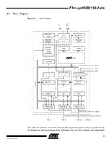
VCCGND WatchdogTimer PowerSupervisionPOR / BOD &RESET debugWIRE WatchdogOscillator > PROGRAMLOGIC OscillatorCircuits /ClockGeneration Flash SRAM CPU EEPROM > GNDAREFAVCC 8bit T/C 0 16bit T/C 1 A/D Conv. > 2 8bit T/C 2 AnalogComp. InternalBandgap > 6 DATABUS USART 0 SPI TWI PORT D (8) PORT B (8) PORT C (7) > RESET XTAL[1..2] ADC[6..7]PC[0..6]PB[0..7]PD[0..7]
Open the catalog to page 3
registers to be accessed in one single instruction executed in one clock cycle. The resulting architecture is more code efficient while achieving throughputs up to ten times faster than con-ventional CISC microcontrollers.The ATmega48/88/168 provides the following features: 4K/8K/16K bytes of In-System Program-mable Flash with Read-While-Write capabilities, 256/512/512 bytes EEPROM, 512/1K/1K bytes SRAM, 23 general purpose I/O lines, 32 general purpose working registers, three flexible Timer/Counters with compare modes, internal and external interrupts, a serial programmable USART, a byte-oriented...
Open the catalog to page 4
Depending on the clock selection fuse settings, PB7 can be used as output from the inverting Oscillator amplifier.If the Internal Calibrated RC Oscillator is used as chip clock source, PB7..6 is used as TOSC2..1 input for the Asynchronous Timer/Counter2 if the AS2 bit in ASSR is set.The various special features of Port B are elaborated in Alternate Functions of Port BӔ on page 69 and System Clock and Clock OptionsӔ on page 24. 3.4.4Port C (PC5..0) Port C is a 7-bit bi-directional I/O port with internal pull-up resistors (selected for each bit). The PC5..0 output buffers have symmetrical drive...
Open the catalog to page 6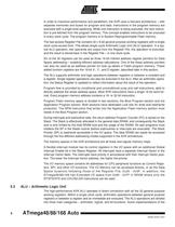
In order to maximize performance and parallelism, the AVR uses a Harvard architecture with separate memories and buses for program and data. Instructions in the program memory are executed with a single level pipelining. While one instruction is being executed, the next instruc- tion is pre-fetched from the program memory. This concept enables instructions to be executed in every clock cycle. The program memory is In-System Reprogrammable Flash memory.The fast-access Register File contains 32 x 8-bit general purpose working registers with a single clock cycle access time. This allows single-cycle...
Open the catalog to page 8
Figure 5-4 shows the parallel instruction fetches and instruction executions enabled by the Har-vard architecture and the fast-access Register File concept. This is the basic pipelining concept to obtain up to 1 MIPS per MHz with the corresponding unique results for functions per cost, functions per clocks, and functions per power-unit. Figure 5-4. The Parallel Instruction Fetches and Instruction Executions Figure 5-5 shows the internal timing concept for the Register File. In a single clock cycle an ALU operation using two register operands is executed, and the result is stored back to the destina-tion...
Open the catalog to page 12
in r16, SREG ; store SREG value cli ; disable interrupts during timed sequence sbi EECR, EEMPE ; start EEPROM write sbi EECR, EEPE out SREG, r16 ; restore SREG value (I-bit) > char cSREG;cSREG = SREG; /* store SREG value */ /* disable interrupts during timed sequence */ _CLI(); EECR |= (1<
Open the catalog to page 13
sei ; set Global Interrupt Enable sleep ; enter sleep, waiting for interrupt ; note: will enter sleep before any pending interrupt(s) > __enable_interrupt(); /* set Global Interrupt Enable */ __sleep(); /* enter sleep, waiting for interrupt */ /* note: will enter sleep before any pending interrupt(s) */ >
Open the catalog to page 14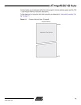
Constant tables can be allocated within the entire program memory address space (see the LPM Load Program Memory instruction description).Timing diagrams for instruction fetch and execution are presented in ֓Instruction Execution Tim-ing on page 11. Figure 6-1. Program Memory Map, ATmega48 > 0x0000 0x7FF Program Memory Application Flash Section 15 > 7530GԖAVR10/07 size="-2">
Open the catalog to page 15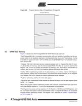
Figure 6-2. Program Memory Map, ATmega88 and ATmega168 > 0x0000 0x0FFF/0x1FFF Program Memory Application Flash Section Boot Flash Section Figure 6-3 shows how the ATmega48/88/168 SRAM Memory is organized.The ATmega48/88/168 is a complex microcontroller with more peripheral units than can be sup-ported within the 64 locations reserved in the Opcode for the IN and OUT instructions. For the Extended I/O space from 0x60 - 0xFF in SRAM, only the ST/STS/STD and LD/LDS/LDD instruc-tions can be used. The lower 768/1280/1280 data memory locations address both the Register File, the I/O mem-ory, Extended...
Open the catalog to page 16All Atmel catalogs and technical brochures
 32-bit Microcontrollers
20 Pages
 MCUs Driving Displays
12 Pages
 Touch and 3D Gesture Control
12 Pages
 16-bit MCUs and DSCs
20 Pages
 XLP PIC® MCUs
8 Pages
 8-bit MCUs
16 Pages
 AT93C56B/66B Automotive
17 Pages
 Atmel AT86RF215 Device Family
235 Pages
 AT24C01C/02C
22 Pages
 maXTouch U Series - Flyer
2 Pages


Archived catalogs
 tinyAVR ATtiny24/44/84 Preliminary
240 Pages
 ATmega164P/324P/644P Preliminary
440 Pages
 ATmega48P/88P/168P/328P Preliminary
426 Pages
 ATmega1284P Preliminary
356 Pages
 AT90PWM216/316
359 Pages
 AT90PWM2, AT90PWM3, AT90PWM2B, AT90PWM3B
361 Pages
 ATmega329/3290/649/6490 Preliminary
392 Pages
 ATmega329P/3290P Preliminary
388 Pages
 AT90CAN32/64/128
428 Pages
 AT86RF230 Preliminary
98 Pages
 ATtiny25, ATtiny45, ATtiny85 Automotive
192 Pages
 ATtiny24/44/84 Automotive Preliminary
225 Pages
 AT86RF231 Preliminary
180 Pages
 Biometrics (Fingerprint Sensor)
20 Pages


- Transceiver module
- Potentiometer
- Industrial converter
- Ethernet transceiver
- Analog potentiometer
- Low-noise amplifier
- Analog amplifier
- Analog converter
- Circuit board
- Operational amplifier
- 32-bit microcontroller
- Low-power microcontroller
- Analog microcontroller
- High-speed converter
- General purpose microcontroller
- DAC converter
- Communication microcontroller
- High-speed amplifier
- ARM microcontroller