ATmega329P/3290P Preliminary
1 /388Pages

ATmega329P/3290P Preliminary
1 /388Pages
Catalog excerpts
High Performance, Low Power AVR > ծ 8-Bit Microcontroller > Advanced RISC Architecture130 Powerful Instructions ֖ Most Single Clock Cycle Execution32 x 8 General Purpose Working Registers ֖Fully Static OperationUp to 20 MIPS Throughput at 20 MHz֖On-Chip 2-cycle Multiplier > High Endurance Non-volatile Memory segments32K Bytes of In-System Self-programmable Flash program memory֖1024 Bytes EEPROM2K Bytes Internal SRAM ֖Write/Erase cyles: 10,000 Flash/100,000 EEPROM > (1)(3) Data retention: 20 years at 85ְC/100 years at 25C > (2)(3) ЖOptional Boot Code Section with Independent Lock BitsIn-System Programming by On-chip Boot ProgramTrue Read-While-Write OperationProgramming Lock for Software Security > JTAG (IEEE std. 1149.1 compliant) Interface֖Boundary-scan Capabilities According to the JTAG StandardExtensive On-chip Debug Support ֖Programming of Flash, EEPROM, Fuses, and Lock Bits through the JTAG Interface > Peripheral Features4 x 25 Segment LCD Driver (ATmega329P) ֖4 x 40 Segment LCD Driver (ATmega3290P)Two 8-bit Timer/Counters with Separate Prescaler and Compare Mode֖One 16-bit Timer/Counter with Separate Prescaler, Compare Mode, and Capture ModeReal Time Counter with Separate Oscillator֖Four PWM Channels 8-channel, 10-bit ADC֖Programmable Serial USARTMaster/Slave SPI Serial Interface ֖Universal Serial Interface with Start Condition DetectorProgrammable Watchdog Timer with Separate On-chip Oscillator֖On-chip Analog Comparator Interrupt and Wake-up on Pin Change > Special Microcontroller Features֖Power-on Reset and Programmable Brown-out Detection Internal Calibrated Oscillator֖External and Internal Interrupt SourcesFive Sleep Modes: Idle, ADC Noise Reduction, Power-save, Power-down, and Standby > I/O and Packages֖54/69 Programmable I/O Lines 64-lead TQFP, 64-pad QFN/MLF, and 100-lead TQFP > Ultra-Low Power ConsumptionActive Mode: 420ֵA at 1 MHz, 1.8VPower-down Mode: 40 nA at 1.8V֖Power-save Mode: 750 nA at 1.8V Notes:1.Worst case temperature. Guaranteed after last write cycle.2.Failure rate less than 1 ppm.3.Characterized through accelerated tests. > 8021CAVR֖08/07 size="-1">
Open the catalog to page 1
The following section describes the I/O-pin special functions. 2.3.1V > CC Digital supply voltage. 2.3.2GND Ground. 2.3.3Port A (PA7..PA0) Port A is an 8-bit bi-directional I/O port with internal pull-up resistors (selected for each bit). ThePort A output buffers have symmetrical drive characteristics with both high sink and sourcecapability. As inputs, Port A pins that are externally pulled low will source current if the pull-up resistors are activated. The Port A pins are tri-stated when a reset condition becomes active,even if the clock is not running.Port A also serves the functions of various...
Open the catalog to page 6
2.3.7Port E (PE7..PE0) Port E is an 8-bit bi-directional I/O port with internal pull-up resistors (selected for each bit). ThePort E output buffers have symmetrical drive characteristics with both high sink and sourcecapability. As inputs, Port E pins that are externally pulled low will source current if the pull-upresistors are activated. The Port E pins are tri-stated when a reset condition becomes active,even if the clock is not running.Port E also serves the functions of various special features of the ATmega329P/3290P as listedon page 79. 2.3.8Port F (PF7..PF0) Port F serves as the analog...
Open the catalog to page 7
2.3.12RESET Reset input. A low level on this pin for longer than the minimum pulse length will generate areset, even if the clock is not running. The minimum pulse length is given in System and ResetCharacteristicsԔ on page 332. Shorter pulses are not guaranteed to generate a reset. 2.3.13XTAL1 Input to the inverting Oscillator amplifier and input to the internal clock operating circuit. 2.3.14XTAL2 Output from the inverting Oscillator amplifier. 2.3.15AVCC AVCC is the supply voltage pin for Port F and the A/D Converter. It should be externally con-nected to V > CC , even if the ADC is not used....
Open the catalog to page 8
A comprehensive set of development tools, application notes and datasheets are available fordownload on http://www.atmel.com/avr. 9 > 8021CAVR֖08/07 size="-1">
Open the catalog to page 9
This documentation contains simple code examples that briefly show how to use various parts ofthe device. These code examples assume that the part specific header file is included beforecompilation. Be aware that not all C compiler vendors include bit definitions in the header filesand interrupt handling in C is compiler dependent. Please confirm with the C compiler documen-tation for more details.For I/O Registers located in extended I/O map, INӔ, OUTӔ, SBISӔ, SBICӔ, CBIӔ, and SBIӔinstructions must be replaced with instructions that allow access to extended I/O. TypicallyLDSӔ and STSӔ combined...
Open the catalog to page 10
ical ALU operation, two operands are output from the Register File, the operation is executed,and the result is stored back in the Register File in one clock cycle.Six of the 32 registers can be used as three 16-bit indirect address register pointers for DataSpace addressing ֖ enabling efficient address calculations. One of the these address pointerscan also be used as an address pointer for look up tables in Flash program memory. Theseadded function registers are the 16-bit X-, Y-, and Z-register, described later in this section.The ALU supports arithmetic and logic operations between registers...
Open the catalog to page 12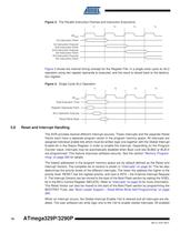
T1T2T3T4 clk1st Instruction Fetch1st Instruction Execute2nd Instruction Fetch > CPU 2 nd Instruction Execute3rd Instruction Fetch3rd Instruction Execute4th Instruction Fetch > T1T2T3T4 clk > CPU Total Execution Time R egister Operands FetchALU Operation ExecuteResult Write Back >
Open the catalog to page 16
in r16, SREG ; store SREG value cli ; disable interrupts during timed sequence sbi EECR, EEMWE ; start EEPROM write sbi EECR, EEWE out SREG, r16 ; restore SREG value (I-bit) > char cSREG;cSREG = SREG; /* store SREG value */ /* disable interrupts during timed sequence */ __disable_interrupt(); EECR |= (1<
Open the catalog to page 17
sei ; set Global Interrupt Enable sleep ; enter sleep, waiting for interrupt ; note: will enter sleep before any pending ; interrupt(s) > __enable_interrupt(); /* set Global Interrupt Enable */ __sleep(); /* enter sleep, waiting for interrupt */ /* note: will enter sleep before any pending interrupt(s) */ >
Open the catalog to page 18All Atmel catalogs and technical brochures
 32-bit Microcontrollers
20 Pages
 MCUs Driving Displays
12 Pages
 Touch and 3D Gesture Control
12 Pages
 16-bit MCUs and DSCs
20 Pages
 XLP PIC® MCUs
8 Pages
 8-bit MCUs
16 Pages
 AT93C56B/66B Automotive
17 Pages
 Atmel AT86RF215 Device Family
235 Pages
 AT24C01C/02C
22 Pages
 maXTouch U Series - Flyer
2 Pages


Archived catalogs
 tinyAVR ATtiny24/44/84 Preliminary
240 Pages
 ATmega164P/324P/644P Preliminary
440 Pages
 ATmega48P/88P/168P/328P Preliminary
426 Pages
 ATmega1284P Preliminary
356 Pages
 AT90PWM216/316
359 Pages
 AT90PWM2, AT90PWM3, AT90PWM2B, AT90PWM3B
361 Pages
 ATmega329/3290/649/6490 Preliminary
392 Pages
 AT90CAN32/64/128
428 Pages
 AT86RF230 Preliminary
98 Pages
 ATmega48/88/168 Automotive
335 Pages
 ATtiny25, ATtiny45, ATtiny85 Automotive
192 Pages
 ATtiny24/44/84 Automotive Preliminary
225 Pages
 AT86RF231 Preliminary
180 Pages
 Biometrics (Fingerprint Sensor)
20 Pages


- Transceiver module
- Potentiometer
- Industrial converter
- Ethernet transceiver
- Analog potentiometer
- Low-noise amplifier
- Analog amplifier
- Analog converter
- Circuit board
- Operational amplifier
- 32-bit microcontroller
- Low-power microcontroller
- Analog microcontroller
- High-speed converter
- General purpose microcontroller
- DAC converter
- Communication microcontroller
- High-speed amplifier
- ARM microcontroller