ATmega329/3290/649/6490 Preliminary
1 /392Pages

ATmega329/3290/649/6490 Preliminary
1 /392Pages
Catalog excerpts

The AVR core combines a rich instruction set with 32 general purpose working registers. All the32 registers are directly connected to the Arithmetic Logic Unit (ALU), allowing two independentregisters to be accessed in one single instruction executed in one clock cycle. The resultingarchitecture is more code efficient while achieving throughputs up to ten times faster than con-ventional CISC microcontrollers.The ATmega329/3290/649/6490 provides the following features: 32/64K bytes of In-SystemProgrammable Flash with Read-While-Write capabilities, 1/2K bytes EEPROM, 2/4K byte SRAM, 54/69 general...
Open the catalog to page 5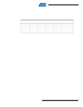
The ATmega329, ATmega3290, ATmega649, and ATmega6490 differs only in memory sizes,pin count and pinout. Table 3-1 on page 6 summarizes the different configurations for the fourdevices. Table 3-1. Configuration Summary > DeviceFlashEEPROMRAMLCD SegmentsGeneral PurposeI/O Pins ATmega32932K bytes1K bytes2K bytes4 x 2554ATmega329032K bytes1K bytes2K bytes4 x 4069ATmega64964K bytes2K bytes4K bytes4 x 2554ATmega649064K bytes2K bytes4K bytes4 x 4069 The following section describes the I/O-pin special functions. 3.3.1V > CC Digital supply voltage. 3.3.2GND Ground. 3.3.3Port A (PA7..PA0) Port A is an...
Open the catalog to page 6
3.3.5Port C (PC7..PC0) Port C is an 8-bit bi-directional I/O port with internal pull-up resistors (selected for each bit). ThePort C output buffers have symmetrical drive characteristics with both high sink and sourcecapability. As inputs, Port C pins that are externally pulled low will source current if the pull-upresistors are activated. The Port C pins are tri-stated when a reset condition becomes active,even if the clock is not running.Port C also serves the functions of special features of the ATmega329/3290/649/6490 as listedon page 71. 3.3.6Port D (PD7..PD0) Port D is an 8-bit bi-directional...
Open the catalog to page 7
3.3.9Port G (PG5..PG0) Port G is a 6-bit bi-directional I/O port with internal pull-up resistors (selected for each bit). ThePort G output buffers have symmetrical drive characteristics with both high sink and sourcecapability. As inputs, Port G pins that are externally pulled low will source current if the pull-upresistors are activated. The Port G pins are tri-stated when a reset condition becomes active, even if the clock is not running.Port G also serves the functions of various special features of the ATmega329/3290/649/6490as listed on page 75. 3.3.10Port H (PH7..PH0) Port H is a 8-bit...
Open the catalog to page 8
3.3.17LCDCAP An external capacitor (typical > 470 nF) must be connected to the LCDCAP pin as shown in Fig-ure 24-2. This capacitor acts as a reservoir for LCD power (V > LCD ). A large capacitance reducesripple on V > LCD but increases the time until V > LCD reaches its target value. > A comprehensive set of development tools, application notes and datasheets are available for download on http://www.atmel.com/avr. > Note:1. Reliability Qualification results show that the projected data retention failure rate is much less than 1 PPM over 20 years at 85C or 100 years at 25аC. > This documentation...
Open the catalog to page 9
The fast-access Register File contains 32 x 8-bit general purpose working registers with a singleclock cycle access time. This allows single-cycle Arithmetic Logic Unit (ALU) operation. In a typ-ical ALU operation, two operands are output from the Register File, the operation is executed,and the result is stored back in the Register File in one clock cycle.Six of the 32 registers can be used as three 16-bit indirect address register pointers for DataSpace addressing ֖ enabling efficient address calculations. One of the these address pointerscan also be used as an address pointer for look up tables...
Open the catalog to page 11
This section describes the general access timing concepts for instruction execution. The AVRCPU is driven by the CPU clock clk > CPU , directly generated from the selected clock source for thechip. No internal clock division is used.Figure 7-4 shows the parallel instruction fetches and instruction executions enabled by the Har-vard architecture and the fast-access Register File concept. This is the basic pipelining conceptto obtain up to 1 MIPS per MHz with the corresponding unique results for functions per cost, functions per clocks, and functions per power-unit. Figure 7-4. The Parallel Instruction...
Open the catalog to page 15
in r16, SREG ; store SREG value cli ; disable interrupts during timed sequence sbi EECR, EEMWE ; start EEPROM write sbi EECR, EEWE out SREG, r16 ; restore SREG value (I-bit) > char cSREG;cSREG = SREG; /* store SREG value */ /* disable interrupts during timed sequence */ __disable_interrupt(); EECR |= (1<
Open the catalog to page 16
sei ; set Global Interrupt Enable sleep ; enter sleep, waiting for interrupt ; note: will enter sleep before any pending ; interrupt(s) > __enable_interrupt(); /* set Global Interrupt Enable */ __sleep(); /* enter sleep, waiting for interrupt */ /* note: will enter sleep before any pending interrupt(s) */ >
Open the catalog to page 17
This section describes the different memories in the ATmega329/3290/649/6490. The AVRarchitecture has two main memory spaces, the Data Memory and the Program Memory space.In addition, the ATmega329/3290/649/6490 features an EEPROM Memory for data storage. Allthree memory spaces are linear. > The ATmega329/3290/649/6490 contains 32/64K bytes On-chip In-System ReprogrammableFlash memory for program storage. Since all AVR instructions are 16 or 32 bits wide, the Flashis organized as 16/32K x 16. For software security, the Flash Program memory space is dividedinto two sections, Boot Program section...
Open the catalog to page 18
Figure 8-2 shows how the ATmega329/3290/649/6490 SRAM Memory is organized.The ATmega329/3290/649/6490 is a complex microcontroller with more peripheral units thancan be supported within the 64 locations reserved in the Opcode for the IN and OUT instruc-tions. For the Extended I/O space from 0x60 - 0xFF in SRAM, only the ST/STS/STD andLD/LDS/LDD instructions can be used. The lower 2304/4352 data memory locations address both the Register File, the I/O memory,Extended I/O memory, and the internal data SRAM. The first 32 locations address the RegisterFile, the next 64 location the standard I/O memory,...
Open the catalog to page 19All Atmel catalogs and technical brochures
 32-bit Microcontrollers
20 Pages
 MCUs Driving Displays
12 Pages
 Touch and 3D Gesture Control
12 Pages
 16-bit MCUs and DSCs
20 Pages
 XLP PIC® MCUs
8 Pages
 8-bit MCUs
16 Pages
 AT93C56B/66B Automotive
17 Pages
 Atmel AT86RF215 Device Family
235 Pages
 AT24C01C/02C
22 Pages
 maXTouch U Series - Flyer
2 Pages


Archived catalogs
 tinyAVR ATtiny24/44/84 Preliminary
240 Pages
 ATmega164P/324P/644P Preliminary
440 Pages
 ATmega48P/88P/168P/328P Preliminary
426 Pages
 ATmega1284P Preliminary
356 Pages
 AT90PWM216/316
359 Pages
 AT90PWM2, AT90PWM3, AT90PWM2B, AT90PWM3B
361 Pages
 ATmega329P/3290P Preliminary
388 Pages
 AT90CAN32/64/128
428 Pages
 AT86RF230 Preliminary
98 Pages
 ATmega48/88/168 Automotive
335 Pages
 ATtiny25, ATtiny45, ATtiny85 Automotive
192 Pages
 ATtiny24/44/84 Automotive Preliminary
225 Pages
 AT86RF231 Preliminary
180 Pages
 Biometrics (Fingerprint Sensor)
20 Pages


- Transceiver module
- Potentiometer
- Industrial converter
- Ethernet transceiver
- Analog potentiometer
- Low-noise amplifier
- Analog amplifier
- Analog converter
- Circuit board
- Operational amplifier
- 32-bit microcontroller
- Low-power microcontroller
- Analog microcontroller
- High-speed converter
- General purpose microcontroller
- DAC converter
- Communication microcontroller
- High-speed amplifier
- ARM microcontroller