ATA6823C H-Bridge Gate-Driver with LIN Transceiver 2.0, Window Watchdog and 3.3/5V Voltage Regulator
1 /26Pages

ATA6823C H-Bridge Gate-Driver with LIN Transceiver 2.0, Window Watchdog and 3.3/5V Voltage Regulator
1 /26Pages
Catalog excerpts

ATA6823C H-bridge Motor Driver DATASHEET Features ● PWM and direction-controlled driving of four externally-powered NMOS transistors ● A programmable dead time is included to avoid peak currents within the H-bridge ● Integrated charge pump to provide gate voltages for high-side drivers and to supply the gate of the external battery reverse protection NMOS ● 5V/3.3V regulator and current limitation function ● Reset derived from 5V/3.3V regulator output voltage ● Sleep mode with supply current of typically < 45µA, wake-up by signal on pins EN2 or on LIN interface ● A programmable window watchdog ● Battery overvoltage protection and battery undervoltage management ● Overtemperature warning and protection (shutdown) ● LIN 2.1 compliant ● 3.3V/5V regulator with trimmed band gap ● QFN32 package
Open the catalog to page 1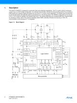
Description The Atmel® ATA6823C is designed for automotive body and powertrain applications. The IC is used to drive a continuous current motor in a full H-bridge configuration. An external microcontroller controls the driving function of the IC by providing a PWM signal and a direction signal and allows the use of the IC in a motor-control application. The PWM control is performed by the low-side switch; the high-side switch is permanently on in the driving phase. The VMODE configuration pin can be set to 5V or 3.3V mode (for regulator and interface high level). The window watchdog has a programmable...
Open the catalog to page 2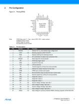
EN2 VBATSW VBAT VCC PGND L1 L2 PBAT VMODE VINT RWD CC /RESET WD GND LIN VG CPLO CPHI VRES H2 S2 H1 S1 YWW Date code (Y = Year - above 2000, WW = week number) ATA6823 Product name ZZZZZ Wafer lot number AL Assembly sub-lot number RC combination to adjust cross conduction time Reset signal for microcontroller Watchdog trigger signal Ground for chip core Transmit signal to LIN bus from microcontroller Defines the rotation direction for the motor PWM input controls motor speed Microcontroller output to keep the chip in active mode Receive signal from LIN bus for microcontroller Source voltage H-bridge,...
Open the catalog to page 3
Power supply (after reverse protection) for charge pump and H-bridge Gate voltage H-bridge, low-side 2 Gate voltage H-bridge, low-side 1 Power ground for H-bridge and charge pump 5V/100 mA supply for microcontroller, blocking capacitor 2.2µF/10V/X7R Supply voltage for IC core (after reverse protection) 100Ω PMOS switch from VVBAT Enable input Function Charge pump capacitor 220nF/25V/X7R Blocking capacitor 470nF/25V/X7R
Open the catalog to page 4
Functional Description Power Supply Unit with Supervisor Functions Power Supply The IC is supplied by a reverse-protected battery voltage. To prevent it from destruction, proper external protection circuitry has to be added. It is recommended to use at least a capacitor combination of storage and HF caps behind the reverse protection circuitry and closed to the VBAT pin of the IC (see Figure 1-1 on page 2). A fully-internal low-power and low-drop regulator, stabilized by an external blocking capacitor provides the necessary lowvoltage supply needed for the wake-up process. The low-power band...
Open the catalog to page 5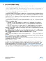
Wake-up and Sleep Mode Strategy The IC has two modes: Sleep and Active. The change between the modes is described below. The default state after power-on is active mode. The wake-up procedure brings the IC from a standby mode (sleep) to an active mode (active). The internal 5V supply VINT, the EN2 pin input structure and a certain part of the LIN receiver are permanently active to ensure a proper startup of the system. The Go to Active and Go to Sleep procedures are implemented as follows: ● Go to Active by activating pin EN2 The input EN2 is intended as a switch-on pin from an external signal....
Open the catalog to page 6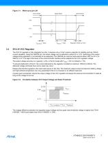
Figure 3-1. Wake-up by pin LIN Active Mode Sleep Mode Active Mode Regulator Wake-up Time 5V/3.3V VCC Regulator The 5V/3.3V regulator is fully integrated on-chip. It requires only a 2.2µF ceramic capacitor for stability and has 100mA current capability. Using the VMODE pin, the output voltage can be selected to either 5V or 3.3V. Switching of the output voltage during operation is not intended to be supported. The VMODE pin must be hard-wired to either VINT for 5V or to GND for 3.3V. The logic HIGH level of the microcontroller interface will be adapted to the VCC regulator voltage. The output...
Open the catalog to page 7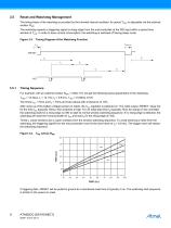
Reset and Watchdog Management The timing basis of the watchdog is provided by the trimmed internal oscillator. Its period TOSC is adjustable via the external resistor RWD. The watchdog expects a triggering signal (a rising edge) from the microcontroller at the WD input within a period time window of TWD. In order to save current consumption, the watchdog is switched off during sleep mode. Figure 3-3. Timing Diagram of the Watchdog Function tresshort tres /RESET Timing Sequence For example, with an external resistor RWD = 33kΩ ±1% we get the following typical parameters of the watchdog. TOSC =...
Open the catalog to page 8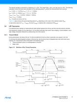
The internal oscillator is trimmed to a tolerance of < ±10%. This means that t1 and t2 can also vary by ±10%. The following calculation shows the worst case calculation of the watchdog period Twd which the microcontroller has to provide. t1min = 0.90 × t1 = 10.87ms, t1max = 1.10 × t1 = 13.28ms t2min = 0.90 × t2 = 8.65ms, t2max = 1.10 × t2 = 10.57ms Twdmax = t1min + t2min = 10.87ms + 8.65ms = 19.52ms Twdmin = t1max = 13.28ms Twd = 16.42ms ±3.15ms (±19.1%) Figure 3-4 above shows the typical watchdog period TWD depending on the value of the external resistor ROSC. A reset will be active for VCC...
Open the catalog to page 9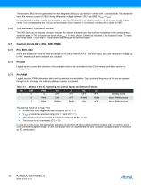
The recessive BUS level is generated from the integrated 30kΩ pull-up resistor in series with an active diode. This diode prevents the reverse current of VBUS during differential voltage between VSUP and BUS (VBUS > VSUP). No additional termination resistor is necessary to use the ATA6823C in LIN slave nodes. If this IC is used for LIN master nodes, it is necessary that the BUS pin be terminated via an external 1 kΩ resistor in series with a diode to VBAT. TXD Dominant Time-out Function The TXD input has an internal pull-down resistor. An internal timer prevents the bus line from being driven...
Open the catalog to page 10All Atmel catalogs and technical brochures
 32-bit Microcontrollers
20 Pages
 MCUs Driving Displays
12 Pages
 Touch and 3D Gesture Control
12 Pages
 16-bit MCUs and DSCs
20 Pages
 XLP PIC® MCUs
8 Pages
 8-bit MCUs
16 Pages
 AT93C56B/66B Automotive
17 Pages
 Atmel AT86RF215 Device Family
235 Pages
 AT24C01C/02C
22 Pages
 maXTouch U Series - Flyer
2 Pages


Archived catalogs
 tinyAVR ATtiny24/44/84 Preliminary
240 Pages
 ATmega164P/324P/644P Preliminary
440 Pages
 ATmega48P/88P/168P/328P Preliminary
426 Pages
 ATmega1284P Preliminary
356 Pages
 AT90PWM216/316
359 Pages
 AT90PWM2, AT90PWM3, AT90PWM2B, AT90PWM3B
361 Pages
 ATmega329/3290/649/6490 Preliminary
392 Pages
 ATmega329P/3290P Preliminary
388 Pages
 AT90CAN32/64/128
428 Pages
 AT86RF230 Preliminary
98 Pages
 ATmega48/88/168 Automotive
335 Pages
 ATtiny25, ATtiny45, ATtiny85 Automotive
192 Pages
 ATtiny24/44/84 Automotive Preliminary
225 Pages
 AT86RF231 Preliminary
180 Pages
 Biometrics (Fingerprint Sensor)
20 Pages


- Transceiver module
- Potentiometer
- Industrial converter
- Ethernet transceiver
- Analog potentiometer
- Low-noise amplifier
- Analog amplifier
- Analog converter
- Circuit board
- Operational amplifier
- 32-bit microcontroller
- Low-power microcontroller
- Analog microcontroller
- High-speed converter
- General purpose microcontroller
- DAC converter
- Communication microcontroller
- High-speed amplifier
- ARM microcontroller