ATA6662C LIN Transceiver, Physical Layer According to Specification 2.1
1 /18Pages

ATA6662C LIN Transceiver, Physical Layer According to Specification 2.1
1 /18Pages
Catalog excerpts

Features ● Operating range from 5V to 27V ● Baud rate up to 20Kbaud ● Improved slew rate control according to LIN specification 2.0, 2.1 and SAEJ2602-2 ● Fully compatible with 3.3V and 5V devices ● Dominant time-out function at transmit data (TXD) ● Normal and Sleep Mode ● Wake-up capability via LIN Bus (90µs dominant) ● External wake-up via WAKE pin (35µs low level) ● Control of external voltage regulator via INH pin ● Very low standby current during sleep mode (10µA) ● Wake-up source recognition ● Bus pin short-circuit protected versus GND and battery ● LIN input current < 2µA if VBAT is disconnected ● Overtemperature protection ● High EMC level ● Interference and damage protection according to ISO/CD 7637 ● Fulfills the OEM “Hardware Requirements for LIN in Automotive Applications Rev.1.0”
Open the catalog to page 1
Description The Atmel® ATA6662C is a fully integrated LIN transceiver complying with the LIN specification 2.0, 2.1 and SAEJ2602-2. It interfaces the LIN protocol handler and the physical layer. The device is designed to handle the low-speed data communication in vehicles, for example, in convenience electronics. Improved slope control at the LIN driver ensures secure data communication up to 20Kbaud. Sleep Mode guarantees minimal current consumption. The Atmel ATA6662C has advanced EMI and ESD performance. Figure 1-1. Block Diagram 7 Short circuit and overtemperature protection Slew rate control...
Open the catalog to page 2
Functional Description Physical Layer Compatibility Since the LIN physical layer is independent from higher LIN layers (e.g., the LIN protocol layer), all nodes with a LIN physical layer according to revision 2.x can be mixed with LIN physical layer nodes, which, according to older versions (i.e., LIN 1.0, LIN 1.1, LIN 1.2, LIN 1.3), are without any restrictions. Supply Pin (VS) Undervoltage detection is implemented to disable transmission if VS falls to a value below 5V in order to avoid false bus messages. After switching on VS, the IC switches to Fail-safe Mode and INHIBIT is switched on....
Open the catalog to page 4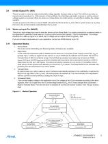
Inhibit Output Pin (INH) This pin is used to control an external switchable voltage regulator having a wake-up input. The inhibit pin provides an internal switch towards pin VS. If the device is in Normal Mode, the inhibit high-side switch is turned on and the external voltage regulator is activated. When the device is in Sleep Mode, the inhibit switch is turned off and disables the voltage regulator. A wake-up event on the LIN bus or at pin WAKE will switch the INH pin to the VS level. After a system power-up (VS rises from zero), the pin INH switches automatically to the VS level. Wake-up Input...
Open the catalog to page 5
High, except after wake up High ohmic Wake-up events from Sleep Mode: ● LIN bus Figure 3-1 on page 5, Figure 3-2 and Figure 3-3 on page 7 show details of wake-up operations. Remote Wake-up via Dominant Bus State A voltage less than the LIN pre-wake detection VLINL at pin LIN activates the internal LIN receiver and switches on the internal slave termination between the LIN pin and the VS pin. A falling edge at pin LIN, followed by a dominant bus level VBUSdom maintained for a certain time period (tBUS) and a rising edge at pin LIN results in a remote wake-up request. The device switches to Fail-safe...
Open the catalog to page 6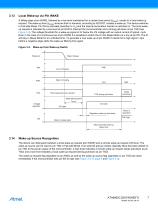
Local Wake-up via Pin WAKE A falling edge at pin WAKE, followed by a low level maintained for a certain time period (tWAKE), results in a local wake-up request. The wake-up time (tWAKE) ensures that no transient, according to ISO7637, creates a wake-up. The device switches to Fail-safe Mode. Pin INH is activated (switches to VS) and the internal termination resistor is switched on. The local wakeup request is indicated by a low level at pin RXD to interrupt the microcontroller and a strong pull-down at pin TXD (see Figure 3-3). The voltage threshold for a wake-up signal is 3V below the VS voltage...
Open the catalog to page 7
Pin EN provides a pull-down resistor to force the transceiver into Sleep Mode if EN is disconnected. The reverse current is < 2µA at pin LIN during loss of VBAT; this is optimal behavior for bus systems where some slave nodes are supplied from battery or ignition. The implemented hysteresis, Thys, enables the LIN output again after the temperature has been decreased. Pin RXD is set floating if VBAT is disconnected. Pin TXD provides a pull-down resistor to provide a static low if TXD is disconnected. The LIN output driver has a current limitation, and if the junction temperature Tj exceeds the...
Open the catalog to page 8
Absolute Maximum Ratings Stresses beyond those listed under “Absolute Maximum Ratings” may cause permanent damage to the device. This is a stress rating only and functional operation of the device at these or any other conditions beyond those indicated in the operational sections of this specification is not implied. Exposure to absolute maximum rating conditions for extended periods may affect device reliability. Parameters VS - Continuous supply voltage Wake DC and transient voltage (with 33-kΩ serial resistor) - Transient voltage due to ISO7637 (coupling 1nF) LIN - DC voltage - Transient voltage...
Open the catalog to page 9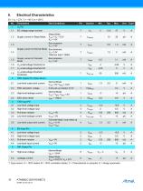
Electrical Characteristics Sleep Mode VLIN > VS – 0.5V VS < 14V Supply current in Normal Mode Bus dominant VS < 14V Total bus load > 500Ω Supply current in Fail-safe Mode VS undervoltage threshold hysteresis Test Conditions DC voltage range nominal Supply current in Sleep Mode RXD Output Pin (Open Drain) Low-level output sink current Normal Mode VLIN = 0V, VRXD = 0.4V High-level leakage current Normal Mode VLIN = VBAT, VRXD = 5V Low-level voltage input High-level voltage input Pull-down resistor Low-level leakage current Low-level output sink current Fail-safe Mode, local wake up VTXD = 0.4V...
Open the catalog to page 10
Electrical Characteristics (Continued) Test Conditions High-level input voltage Low-level input voltage Wake pull-up current High-level leakage current Driver recessive output voltage RLOAD = 500Ω / 1kΩ Driver dominant voltage VBUSdom_DRV_LoSUP Driver dominant voltage VBUSdom_DRV_HiSUP Driver dominant voltage VBUSdom_DRV_LoSUP Driver dominant voltage VBUSdom_DRV_HiSUP The serial diode is mandatory Voltage drop at the serial diodes In pull-up path with Rslave ISerDiode = 10mA LIN current limitation VBUS = VBAT_max Input leakage current at the receiver, including pull-up resistor as specified Driver...
Open the catalog to page 11All Atmel catalogs and technical brochures
 32-bit Microcontrollers
20 Pages
 MCUs Driving Displays
12 Pages
 Touch and 3D Gesture Control
12 Pages
 16-bit MCUs and DSCs
20 Pages
 XLP PIC® MCUs
8 Pages
 8-bit MCUs
16 Pages
 AT93C56B/66B Automotive
17 Pages
 Atmel AT86RF215 Device Family
235 Pages
 AT24C01C/02C
22 Pages
 maXTouch U Series - Flyer
2 Pages


Archived catalogs
 tinyAVR ATtiny24/44/84 Preliminary
240 Pages
 ATmega164P/324P/644P Preliminary
440 Pages
 ATmega48P/88P/168P/328P Preliminary
426 Pages
 ATmega1284P Preliminary
356 Pages
 AT90PWM216/316
359 Pages
 AT90PWM2, AT90PWM3, AT90PWM2B, AT90PWM3B
361 Pages
 ATmega329/3290/649/6490 Preliminary
392 Pages
 ATmega329P/3290P Preliminary
388 Pages
 AT90CAN32/64/128
428 Pages
 AT86RF230 Preliminary
98 Pages
 ATmega48/88/168 Automotive
335 Pages
 ATtiny25, ATtiny45, ATtiny85 Automotive
192 Pages
 ATtiny24/44/84 Automotive Preliminary
225 Pages
 AT86RF231 Preliminary
180 Pages
 Biometrics (Fingerprint Sensor)
20 Pages


- Potentiometer
- Industrial converter
- Ethernet transceiver
- Analog potentiometer
- Low-noise amplifier
- Analog amplifier
- Analog converter
- Circuit board
- Operational amplifier
- 32-bit microcontroller
- Low-power microcontroller
- Analog microcontroller
- High-speed converter
- General purpose microcontroller
- DAC converter
- Communication microcontroller
- High-speed amplifier
- ARM microcontroller