ATA663201/ATA663203/ATA663231/ATA663254
1 /29Pages

ATA663201/ATA663203/ATA663231/ATA663254
1 /29Pages
Catalog excerpts
ATA663201/ATA663203/ATA663231/ATA663254 LIN Bus Device Family including Voltage Regulator and LIN SBC(1) with Compatible Footprint DATASHEET • Supply voltage up to 40V • Operating voltage VS = 5V to 28V • Supply current • Sleep mode: typically 9pA • Silent mode: typically 47pA • Very low current consumption at low supply voltages (2V < VS < 5.5V): typically 130pA • Linear low-drop voltage regulator, 85mA current capability: • MLC (multi-layer ceramic) capacitor with 0Q ESR • Normal, fail-safe, and silent mode • Atmel® ATA663254: VCC = 5.0V ±2% • Atmel ATA663231: VCC = 3.3V ±2% • Sleep mode: VCC is switched off • Active mode • Atmel ATA663203: VCC = 5.0V ±2% • Atmel ATA663201: VCC = 3.3V ±2% • VCC undervoltage detection with open drain reset output (NRES, 4ms reset time) • Voltage regulator is short-circuit and over-temperature protected • LIN physical layer according to LIN 2.0, 2.1,2.2, 2.2A and SAEJ2602-2 • Wake-up capability via LIN bus (100ps dominant) • Wake-up source recognition • TXD time-out timer • Bus pin is over-temperature and short-circuit protected versus GND and battery • Advanced EMC and ESD performance • Fulfills the OEM “Hardware Requirements for LIN in Automotive Applications Rev.1.3” • Interference and damage protection according to ISO7637 • Qualified according to AEC-Q100 • Packages: • DFN8 (all types) with wettable flanks (Moisture Sensitivity Level 1) • SO8 (only Atmel ATA663254) Note: 1. LIN SBC: LIN system basis chip including LIN transceiver and voltage
Open the catalog to page 1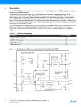
Description The Atmel® ATA6632xx device family includes two basic products; a LIN system basis chip (SBC) and a low-drop voltage regulator with compatible footprints. The Atmel ATA663231/54 (system basis chip) is a fully integrated LIN transceiver, designed according to the LIN specification 2.0, 2.1, 2.2, 2.2A and SAEJ2602-2, with a low-drop voltage regulator (3.3V/5V/85mA). The combination of voltage regulator and bus transceiver makes it possible to develop simple but powerful slave nodes in LIN bus systems. Atmel ATA663231/54 is designed to handle the low-speed data communication in vehicles...
Open the catalog to page 2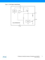
Figure 1-2. Block Diagram Voltage Regulator VS 7 Voltage Reference Undervoltage Reset
Open the catalog to page 3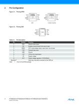
Figure 2-1. Pinning DFN8 RXD EN NRES TXD Voltage regulator Figure 2-2. Pinning SO8 RXD EN NRES TXD Note: 1. Only for the DFN8 package.
Open the catalog to page 4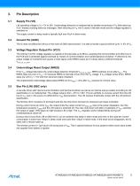
Supply Pin (VS) LIN operating voltage is VS = 5V to 28V. Undervoltage detection is implemented to disable transmission if VS falls below typ. 4.5V, thereby avoiding false bus messages. After switching on VS, the IC starts in fail-safe mode and the voltage regulator is switched on. The supply current in sleep mode is typically 9µA and 47µA in silent mode. Ground Pin (GND) The IC does not affect the LIN bus in the event of GND disconnection. It is able to handle a ground shift of up to 11.5% of VS. Voltage Regulator Output Pin (VCC) The internal 3.3V/5V voltage regulator is capable of driving loads...
Open the catalog to page 5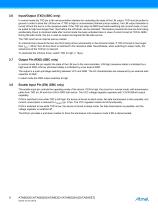
Input/Output (TXD) (SBC only) In normal mode the TXD pin is the microcontroller interface for controlling the state of the LIN output. TXD must be pulled to ground in order to drive the LIN bus low. If TXD is high or unconnected (internal pull-up resistor), the LIN output transistor is turned off and the bus is in the recessive state. If the TXD pin stays at GND level while switching into normal mode, it must be pulled to high level longer than 10µs before the LIN driver can be activated. This feature prevents the bus line from being accidentally driven to dominant state after normal mode has...
Open the catalog to page 6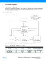
Functional Description Physical Layer Compatibility Because the LIN physical layer is independent of higher LIN layers (e.g., LIN protocol layer), all nodes with a LIN physical layer according to revision 2.x can be mixed with LIN physical layer nodes based on earlier versions (i.e., LIN 1.0, LIN 1.1, LIN 1.2, LIN 1.3) without any restrictions. Operating Modes Figure 4-1. SBC Operating Modes a: VS > VVS_th_U_F_up (2.4V) b: VS < VVS_th_U_down (1.9V) c: Bus wake-up event (LIN) d: VCC < VVCC_th_uv_down (2.4V/4.2V) e: VS < VVS_th_N_F_down (3.9V) f: VS > VVS_th_F_N_up (4.9V) Unpowered Mode All circuitry...
Open the catalog to page 7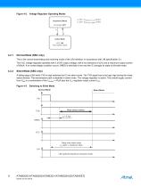
Figure 4-2. Voltage Regulator Operating Modes
Open the catalog to page 8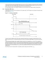
In silent mode the internal slave termination between the LIN pin and VS pin is disabled to minimize the current consumption in case the pin LIN is short-circuited to GND. Only a weak pull-up current (typically 10µA) between the LIN pin and VS pin is present. Silent mode can be activated independently from the current level on pin LIN. If an undervoltage condition occurs, NRES is switched to low and the Atmel® SBC changes its state to fail-safe mode. Sleep Mode (SBC only) A falling edge at EN while TXD is low switches the IC into sleep mode. The TXD signal has to be logic low during the mode...
Open the catalog to page 9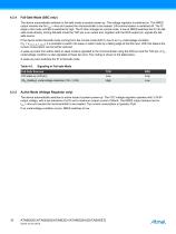
4.2.4 Fail-Safe Mode (SBC only) The device automatically switches to fail-safe mode at system power-up. The voltage regulator is switched on. The NRES output remains low for tres = 4ms and causes the microcontroller to be reseted. LIN communication is switched off. The IC stays in this mode until EN is switched to high. The IC then changes to normal mode. A low at NRES switches the IC into failsafe mode directly. During fail-safe mode the TXD pin is an output and, together with the RXD output pin, signals the failsafe source. If the device enters fail-safe mode coming from the normal mode (EN=1)...
Open the catalog to page 10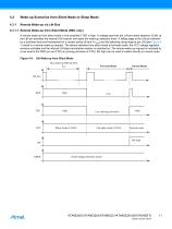
Wake-up Scenarios from Silent Mode or Sleep Mode 4.3.1.1 Remote Wake-up from Silent Mode (SBC only) A remote wake-up from silent mode is only possible if TXD is high. A voltage less than the LIN pre-wake detection VLINL at the LIN pin activates the internal LIN receiver and starts the wake-up detection timer. A falling edge at the LIN pin followed by a dominant bus level maintained for a certain period of time (> tbus) and the following rising edge at pin LIN (see Figure 45) result in a remote wake-up request. The device switches from silent mode to fail-safe mode, the VCC voltage regulator remains...
Open the catalog to page 11All Atmel catalogs and technical brochures
 32-bit Microcontrollers
20 Pages
 MCUs Driving Displays
12 Pages
 Touch and 3D Gesture Control
12 Pages
 16-bit MCUs and DSCs
20 Pages
 XLP PIC® MCUs
8 Pages
 8-bit MCUs
16 Pages
 AT93C56B/66B Automotive
17 Pages
 Atmel AT86RF215 Device Family
235 Pages
 AT24C01C/02C
22 Pages
 maXTouch U Series - Flyer
2 Pages


Archived catalogs
 tinyAVR ATtiny24/44/84 Preliminary
240 Pages
 ATmega164P/324P/644P Preliminary
440 Pages
 ATmega48P/88P/168P/328P Preliminary
426 Pages
 ATmega1284P Preliminary
356 Pages
 AT90PWM216/316
359 Pages
 AT90PWM2, AT90PWM3, AT90PWM2B, AT90PWM3B
361 Pages
 ATmega329/3290/649/6490 Preliminary
392 Pages
 ATmega329P/3290P Preliminary
388 Pages
 AT90CAN32/64/128
428 Pages
 AT86RF230 Preliminary
98 Pages
 ATmega48/88/168 Automotive
335 Pages
 ATtiny25, ATtiny45, ATtiny85 Automotive
192 Pages
 ATtiny24/44/84 Automotive Preliminary
225 Pages
 AT86RF231 Preliminary
180 Pages
 Biometrics (Fingerprint Sensor)
20 Pages


- Potentiometer
- Industrial converter
- Ethernet transceiver
- Analog potentiometer
- Low-noise amplifier
- Analog amplifier
- Analog converter
- Circuit board
- Operational amplifier
- 32-bit microcontroller
- Low-power microcontroller
- Analog microcontroller
- High-speed converter
- General purpose microcontroller
- DAC converter
- Communication microcontroller
- High-speed amplifier
- ARM microcontroller