ATA6629/ATA6631 LIN System Basis Chip with LIN Transceiver and Integrated 3.3V(5V)/50 mA Voltage Regulator
1 /26Pages

ATA6629/ATA6631 LIN System Basis Chip with LIN Transceiver and Integrated 3.3V(5V)/50 mA Voltage Regulator
1 /26Pages
Catalog excerpts

ATA6629/ATA6631 LIN Bus Transceiver with Integrated Voltage Regulator DATASHEET Supply voltage up to 40V Operating voltage VS = 5V to 27V Typically 10µA supply current during sleep mode Typically 35µA supply current in silent mode Linear low-drop voltage regulator, 85mA current capability: ● ● ● ● Normal, fail-safe, and silent mode Atmel ATA6629: VCC = 3.3V ±2% Atmel ATA6631: VCC = 5.0V ±2% Sleep mode: VCC is switched off ● VCC undervoltage detection with reset open drain output NRES (4ms reset time) Voltage regulator is short-circuit and over-temperature protected LIN physical layer according to LIN 2.0, 2.1 and SAEJ2602-2 Wake-up capability via LIN bus (90µs dominant) TXD time-out timer Bus pin is overtemperature and short-circuit protected versus GND and battery Advanced EMC and ESD performance Fulfills the OEM “hardware requirements for LIN in automotive applications rev.1.1” Interference and damage protection according to ISO7637 Package: SO8
Open the catalog to page 1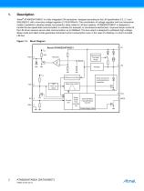
Description Atmel® ATA6629/ATA6631 is a fully integrated LIN transceiver, designed according to the LIN specification 2.0, 2.1 and SAEJ2602-2, with a low-drop voltage regulator (3.3V/5V/85mA). The combination of voltage regulator and bus transceiver makes it possible to develop simple, but powerful, slave nodes in LIN bus systems. ATA6629/ATA6631 is designed to handle the low-speed data communication in vehicles (for example, in convenience electronics). Improved slope control at the LIN driver ensures secure data communication up to 20kBaud. The bus output is designed to withstand high voltage....
Open the catalog to page 2
Symbol Function 2 EN Enables normal mode if the input is high 3 GND Ground, heat sink 5 RXD Receive data output 6 TXD Transmit data input 7 NRES Output undervoltage reset, low at reset 8 VCC Output voltage regulator 3.3V/5V/50mA
Open the catalog to page 3
Functional Description Physical Layer Compatibility Since the LIN physical layer is independent from higher LIN layers (e.g., LIN protocol layer), all nodes with a LIN physical layer according to revision 2.x can be mixed with LIN physical layer nodes, which are according to older versions (i.e., LIN 1.0, LIN 1.1, LIN 1.2, LIN 1.3) without any restrictions. Supply Pin (VS) LIN operating voltage is VS = 5V to 27V. An undervoltage detection is implemented to disable transmission if VS falls below 5V, in order to avoid false bus messages. After switching on VS, the IC starts with the fail-safe mode...
Open the catalog to page 4
Output Pin (RXD) This pin reports the state of the LIN bus to the microcontroller. LIN high (recessive state) is reported by a high level at RXD; LIN low (dominant state) is reported by a low level at RXD. The output has an internal pull-up resistor with typically 5kΩ to VCC. The AC characteristics are measured with an external load capacitor of 20pF. The output is short-circuit protected. In unpowered mode (that is, VS = 0V), RXD is switched off. Enable Input Pin (EN) The enable input pin controls the operation mode of the device. If EN is high, the circuit is in normal mode, with transmission...
Open the catalog to page 5
Modes of Operation Figure 4-1. Modes of Operation a: VS > VSthF Unpowered Mode (See section 4.5) b: VS < VSthU c: Bus wake-up event d: NRES switches to low VCC: 3.3V/5V with undervoltage monitoring Communication: OFF Silent Mode VCC: 3.3V/5V with undervoltage monitoring Communication: OFF Local wake-up event Normal Mode VCC: 3.3V/5V with undervoltage monitoring Sleep Mode Fail safe Normal Mode This is the normal transmitting and receiving mode of the LIN interface, in accordance with LIN specification 2.x. The VCC voltage regulator operates with a 3.3V/5V output voltage, with a low tolerance...
Open the catalog to page 6
Silent Mode A falling edge at EN while TXD is high switches the IC into silent mode. The TXD signal has to be logic high during the mode select window (Figure 4-3 on page 8). The transmission path is disabled in silent mode. The overall supply current from VBatt is a combination of the IVSsilent = 35µA plus the VCC regulator output current IVCC. Figure 4-2. Switch to Silent Mode Normal Mode Silent Mode Mode select window td = 3.2μs Delay time silent mode td_sleep = maximum 20μs LIN LIN switches directly to recessive mode In silent mode the internal slave termination between pin LIN and pin VS...
Open the catalog to page 7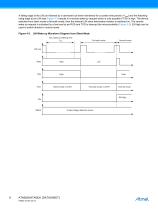
A falling edge at the LIN pin followed by a dominant bus level maintained for a certain time period (> tbus) and the following rising edge at pin LIN (see Figure 4-3) results in a remote wake-up request which is only possible if TXD is high. The device switches from silent mode to fail-safe mode, then the internal LIN slave termination resistor is switched on. The remote wake-up request is indicated by a low level at pin RXD and TXD to interrupt the microcontroller (Figure 4-3). EN high can be used to switch directly to normal mode. Figure 4-3. LIN Wake-up Waveform Diagram from Silent Mode Bus...
Open the catalog to page 8
Sleep Mode A falling edge at EN while TXD is low switches the IC into sleep mode. The TXD signal has to be logic low during the mode select window (Figure 4-5 on page 10). Figure 4-4. Switch to Sleep Mode Sleep Mode Normal Mode Mode select window TXD td = 3.2μs NRES Delay time sleep mode td_sleep = maximum 20μs LIN LIN switches directly to recessive mode In order to avoid any influence to the LIN-pin during switching into sleep mode it is possible to switch the EN up to 3.2µs earlier to low than the TXD. Therefore, the best an easiest way are two falling edges at TXD and EN at the same time....
Open the catalog to page 9
Figure 4-5. LIN Wake-up Diagram from Sleep Mode Bus wake-up filtering time tbus Fail-safe Mode Normal Mode On state Off state Regulator wake-up time EN High EN Reset time NRES Low Microcontroller start-up time delay
Open the catalog to page 10
Sleep or Silent Mode: Behavior at a Floating LIN-bus or a Short Circuited LIN to GND In sleep or in silent mode the device has a very low current consumption even during short-circuits or floating conditions on the bus. A floating bus can arise if the master pull-up resistor is missing, e.g., if it is switched off when the LIN- master is in sleep mode or even if the power supply of the master node is switched off. In order to minimize the current consumption IVS in sleep or silent mode during voltage levels at the LIN-pin below the LIN pre-wake threshold, the receiver is activated only for a...
Open the catalog to page 11All Atmel catalogs and technical brochures
 32-bit Microcontrollers
20 Pages
 MCUs Driving Displays
12 Pages
 Touch and 3D Gesture Control
12 Pages
 16-bit MCUs and DSCs
20 Pages
 XLP PIC® MCUs
8 Pages
 8-bit MCUs
16 Pages
 AT93C56B/66B Automotive
17 Pages
 Atmel AT86RF215 Device Family
235 Pages
 AT24C01C/02C
22 Pages
 maXTouch U Series - Flyer
2 Pages


Archived catalogs
 tinyAVR ATtiny24/44/84 Preliminary
240 Pages
 ATmega164P/324P/644P Preliminary
440 Pages
 ATmega48P/88P/168P/328P Preliminary
426 Pages
 ATmega1284P Preliminary
356 Pages
 AT90PWM216/316
359 Pages
 AT90PWM2, AT90PWM3, AT90PWM2B, AT90PWM3B
361 Pages
 ATmega329/3290/649/6490 Preliminary
392 Pages
 ATmega329P/3290P Preliminary
388 Pages
 AT90CAN32/64/128
428 Pages
 AT86RF230 Preliminary
98 Pages
 ATmega48/88/168 Automotive
335 Pages
 ATtiny25, ATtiny45, ATtiny85 Automotive
192 Pages
 ATtiny24/44/84 Automotive Preliminary
225 Pages
 AT86RF231 Preliminary
180 Pages
 Biometrics (Fingerprint Sensor)
20 Pages


- Potentiometer
- Industrial converter
- Ethernet transceiver
- Analog potentiometer
- Low-noise amplifier
- Analog amplifier
- Analog converter
- Circuit board
- Operational amplifier
- 32-bit microcontroller
- Low-power microcontroller
- Analog microcontroller
- High-speed converter
- General purpose microcontroller
- DAC converter
- Communication microcontroller
- High-speed amplifier
- ARM microcontroller