


ATA6616C/ATA6617C LIN SiP (System-in-Package) Solution Including LIN Transceiver, 5V/50 mA Voltage Regulator, Window Watchdog and AVR ATtiny87 (ATtiny167) Automotive Microcontroller with 8K (16K) Flash Memory

ATA6616C/ATA6617C LIN SiP (System-in-Package) Solution Including LIN Transceiver, 5V/50 mA Voltage Regulator, Window Watchdog and AVR ATtiny87 (ATtiny167) Automotive Microcontroller with 8K (16K) Flash Memory
The ATA6616C/ATA6617C is a high-performance, low-power AVR 8-bit microcontroller with an integrated LIN transceiver, 5V regulator, and watchdog. It features low current consumption in sleep mode, 8K/16K flash memory, supports up to 40V supply voltage, and operates from -40°C to +125°C. It is available in a QFN38 package.
This System-in-Package (SiP) is designed for LIN-bus node applications, combining a LIN-system-basis-chip (LIN-SBC) ATA6624 and an AVR microcontroller (ATtiny87/ATtiny167), offering flexibility similar to discrete components.
Detailed pin descriptions for the QFN38 package are provided, including functions for I/O lines, voltage regulator inputs/outputs, and LIN bus line input/output.
Maximum ratings for the SiP, LIN-SBC, and microcontroller are outlined, including ESD ratings, storage and operating temperatures, and voltage/current limits. Exceeding these ratings may cause permanent damage.
The LIN-SBC supports master and slave operations, with a supply voltage up to 40V and a low-drop voltage regulator with 85mA current capability. It features various modes, wake-up capabilities, and complies with LIN 2.0, 2.1, and SAEJ2602-2 specifications.
Details on physical layer compatibility, supply pin operations, voltage regulator functions, and bus pin characteristics are provided. It describes the functionality of various input/output pins, highlighting their roles in device operation and mode control.
The device operates in several modes: Normal, Silent, Sleep, Fail-safe, and Unpowered, each with specific characteristics regarding VCC, communication, and watchdog status.
Requires external capacitors for stability, with recommendations for capacitor values based on application needs.
Monitors the microcontroller's trigger signals and generates a reset if not received within a specified time window. The timing is adjustable via an external resistor.
The Atmel ATtiny87/ATtiny167 microcontroller features a high-performance, low-power AVR 8-bit architecture with 123 instructions, 8K/16K bytes of flash memory, and various peripheral features including LIN/UART controllers, timers, SPI interfaces, and a 10-bit ADC.
Details on ADC channel pairs, on-chip analog comparator, current source for LIN node identification, on-chip temperature sensor, and programmable watchdog timer are provided. It highlights special features like dynamic clock switching and hardware in-system programmable via SPI Port.
The architecture of the AVR CPU core is outlined, emphasizing its Harvard architecture with separate memories and buses for program and data.
The microcontrollers are developed according to ISO-TS-16949 standards and meet AEC-Q100 grade 1 automotive quality requirements.
Use the comprehensive set of development tools, application notes, and datasheets available on the Atmel website for optimal utilization of the microcontrollers.
The memory size summary table compares the ATtiny87 and ATtiny167, highlighting differences in flash memory size. Block diagrams illustrate the architecture of the AVR CPU and the general-purpose working registers.
The microcontrollers' ability to execute powerful instructions in a single clock cycle is emphasized, achieving high throughput and optimizing power consumption.
The stack pointer in AVR microcontrollers points to the data SRAM stack area, which must be defined before executing subroutine calls or enabling interrupts.
The AVR CPU uses a Harvard architecture for parallel instruction fetches and executions, achieving up to 1 MIPS per MHz.
AVR microcontrollers have multiple interrupt sources, each with a separate program vector. Interrupts are prioritized by their vector address.
The Atmel ATtiny87/167 features three main memory spaces: data memory, program memory, and EEPROM.
Before writing to EEPROM, ensure previous data is erased. During programming, no other EEPROM operations can be performed.
Assembly and C code examples are provided for EEPROM write and read operations.
Low VCC can cause EEPROM data corruption. Keep AVR RESET active during low power supply periods to prevent corruption.
Atmel ATtiny87/167 I/Os and peripherals are in the I/O space.
EEARH and EEARL specify EEPROM address. EEDR contains data for write/read operations.
ATtiny87/167 offers internal and external clock sources. Clock switching should be managed carefully to avoid incorrect configurations.
The internal RC oscillator provides an approximate 8.0MHz clock, nominal at 5V and 25°C.
This low power oscillator provides a 128kHz clock, nominal at 5V and 25°C.
The crystal oscillator can use either a quartz crystal or a ceramic resonator.
This oscillator uses a 32.768kHz watch crystal as the clock source.
The device can be driven by an external clock source.
If not using a crystal oscillator, the system clock can be output on the CLKO pin.
The device features a dynamic clock switch circuit allowing clocks to be turned on and off on the fly.
At reset, bits of the Low Fuse Byte are copied into the CLKSELR register.
Commands are available to enable or disable clock sources.
The system clock can be switched between various sources.
The document outlines the procedure for switching clock sources in the Atmel ATtiny87/167 microcontroller.
Clock monitoring is essential for system safety, covering both peripheral and system clock sources.
The system clock can be divided using the Clock Prescaler Register (CLKPR) to reduce power consumption.
- OSCCAL – Oscillator Calibration Register: Used to trim the internal RC oscillator frequency.
- CLKPR – Clock Prescaler Register: Allows runtime adjustment of clock frequency.
- CLKCSR – Clock Control and Status Register: Manages clock control commands and status.
- CLKSELR – Clock Selection Register: Manages clock source selection and start-up times.
Sleep modes allow the shutdown of unused MCU modules to save power.
The Atmel ATtiny87/167 microcontroller offers four sleep modes: Idle, ADC Noise Reduction, Power-down, and Power-save.
- Idle Mode: Stops the CPU while allowing other peripherals like SPI and ADC to operate.
- ADC Noise Reduction Mode: Halts most clocks except those necessary for ADC operations.
- Power-down Mode: Stops all clocks, allowing only asynchronous modules to operate.
- Power-save Mode: Similar to Power-down but allows Timer/Counter0 to run if clocked asynchronously.
The Brown-out Detector (BOD) can be disabled in certain sleep modes to save power.
To minimize power consumption, unnecessary modules should be disabled.
- SMCR – Sleep Mode Control Register: Controls sleep mode selection and enables sleep mode execution.
- MCUCR – MCU Control Register: Manages BOD settings during sleep.
- PRR – Power Reduction Register: Allows stopping clocks to individual peripherals to save power.
1. PRTIM0: Shuts down Timer/Counter0 in synchronous mode.
Resetting the AVR: During reset, I/O registers are initialized, and the program starts from the reset vector.
The document outlines the configuration of the Watchdog Timer (WDT) in the ATtiny87/167 microcontroller.
The document details the interrupt handling mechanisms in the ATtiny87/167.
External interrupts are managed through several registers.
Pin change interrupts are enabled through PCMSK1 and PCMSK0 registers.
Each bit in PCINT7..0 determines if a pin change interrupt is enabled for the corresponding I/O pin.
AVR ports offer true read-modify-write functionality.
Each port pin has three register bits: DDxn, PORTxn, and PINxn.
When switching a pin from input to output, a tri-state period of one system clock cycle is introduced.
The PINxn register allows reading the pin value.
In sleep modes, digital input signals can be clamped to ground to reduce power consumption.
Port pins may have alternate functions.
- PVOE (Port Value Override Enable): Controls port value via PVOV signal when set.
- PVOV (Port Value Override Value): Sets port value when PVOE is enabled.
- PTOE (Port Toggle Override Enable): Inverts PORTxn register bit when set.
- DIEOE (Digital Input Enable Override Enable): Controls digital input enable via DIEOV signal when set.
- DIEOV (Digital Input Enable Override Value): Enables/disables digital input when DIEOE is set.
- BBMx (Break-Before-Make Mode Enable): Activates break-before-make mode.
- PUDx (Port-Wise Pull-up Disable): Disables port-wise pull-ups.
- Each pin on Port A has multiple alternate functions.
- Similar to Port A, Port B pins have alternate functions.
The output compare (OC0A) function overrides the general I/O port function when COM0A1:0 bits are set.
The COM0A1:0 bits are used differently across normal, CTC, and PWM modes.
The Timer/Counter behavior is defined by the waveform generation mode (WGM01:0) and compare output mode (COM0A1:0) bits.
In normal mode (WGM01:0 = 0), the counter increments and restarts from zero after reaching its maximum value (0xFF).
In CTC mode (WGM01:0 = 2), the counter is cleared when TCNT0 matches OCR0A.
Fast PWM mode (WGM01:0 = 3) generates high-frequency PWM waveforms.
Phase correct PWM mode (WGM01:0 = 1) uses dual-slope operation for high-resolution waveform generation.
Timing diagrams illustrate the Timer/Counter operation.
Switching between asynchronous and synchronous clocking requires careful handling.
The Timer/Counter can be clocked directly by the system clock or through a prescaler.
The Timer/Counter can use an internal clock or an external clock source.
The General Timer/Counter Control Register (GTCCR) includes the Timer/Counter Synchronization Mode (TSM) bit.
The 16-bit Timer/Counter1 supports accurate timing, wave generation, and signal measurement.
The Timer/Counter1 uses 16-bit registers (TCNT1, OCR1A/B, ICR1).
The Timer/Counter can be clocked by internal or external sources.
The document provides a detailed explanation of the Timer/Counter functionalities in a microcontroller.
The counter's behavior is determined by the clock source and mode of operation.
The waveform generation mode bits (WGM13:0) in control registers TCCR1A and TCCR1B dictate the counting sequence and waveform generation.
The input capture unit timestamps external events via the ICP1 pin or an analog comparator.
The noise canceler enhances noise immunity by filtering input signals over four samples.
The 16-bit comparator matches TCNT1 with the output compare register (OCR1A/B).
In non-PWM modes, the match output can be forced without affecting the OCF1A/B flag.
The COM1A/B1:0 bits define the output compare state.
- FOC1A/FOC1B Bits: These bits are active in non-PWM modes.
- TCCR1D Register: Controls output compare pin enable for channels A and B.
- TCNT1H and TCNT1L Registers: Provide direct access to the 16-bit counter.
- OCR1AH/AL and OCR1BH/BL Registers: Contain 16-bit values for output compare.
- ICR1H and ICR1L Registers: Capture counter values on events.
- TIMSK1 Register: Enables various interrupts.
- TIFR1 Register: Contains flags for input capture, output compare, and overflow events.
- Features: Supports full-duplex, three-wire synchronous data transfer.
- Master-Slave Interconnection: Involves shift registers and a master clock generator.
- Master Mode: The SPI clock generator starts with data register writes.
- Slave Mode: The SPI remains passive until the SS pin is low.
- Code Examples: Provided for initializing and using SPI in both master and slave modes.
Master and Slave Configuration:
When the SPI is configured as a master, the SS pin must be held high.
- SPIE: Enables SPI interrupt execution.
- SPE: Enables SPI operations.
- DORD: Determines data order.
- MSTR: Selects master mode.
- CPOL: Sets clock polarity.
- CPHA: Determines if data is sampled on the leading or trailing edge of SCK.
- SPR1, SPR0: Control the SCK rate in master mode.
- SPIF: Set when a serial transfer is complete.
- WCOL: Set if SPDR is written during a data transfer.
- SPI2X: Doubles SPI speed in master mode.
Used for data transfer between the register file and the SPI shift register.
Four combinations of SCK phase and polarity are determined by CPHA and CPOL.
Features: Supports two-wire and three-wire synchronous data transfer.
The document describes the configuration of the Universal Serial Interface (USI) clock and pin position settings.
The document details the Local Interconnect Network (LIN) and Universal Asynchronous Receiver-Transmitter (UART) functionalities.
The LIN protocol involves a master node and multiple slave nodes.
The controller is divided into functions for transmitting and receiving LIN headers and responses.
UART commands are enabled by setting the LCMD[2] bit in the LINENR register.
When enabled, the LRXOK flag indicates an incoming character.
In Tx mode, writing to the LINDAT register sends a character.
The LIN/UART controller resets with the AVR core or via a software reset.
The LBUSY flag indicates active communication.
The baud rate is determined by the system I/O clock frequency and register values.
Data length settings differ between LIN 2.1 and LIN 1.3.
The LINSIR register contains flags indicating successful operations and errors.
A frame time-out error occurs if the frame exceeds the maximum length.
In the event of a frame abortion, the master node is responsible for aborting the ongoing communication.
The checksum is the last field of a frame.
The LINSIR register's communication flags drive two interrupts.
The LIN data buffer operates as a FIFO.
The document provides a detailed description of various LIN/UART registers.
The Atmel ATtiny87/167 features a 100µA constant current source.
During the configuration of a LIN node in a cluster, assigning a unique physical address to each node is necessary.
Tables provide resistor values for 8-address and 16-address systems.
The current source can be used with external transducers.
The AMISCR register controls the current source.
The ATtiny87/167 features a 10-bit ADC with various input channels.
The ADC converts analog input to a digital value.
The ADC requires a clock frequency between 50kHz and 200kHz for maximum resolution.
- Positive Input: The ADC multiplexer can replace the positive input to the analog comparator.
- Negative Input: An internal voltage reference can replace the negative input.
- Features: Includes program flow control, real-time operation, symbolic debugging, and high-speed operation.
- Physical Interface: Activated by programming the DWEN Fuse.
- Software Break Points: Uses the AVR BREAK instruction.
- Limitations: External reset sources are unsupported when debugWIRE is enabled.
- Self-programming: The device can self-program using interfaces like LIN or USART.
- Page Erase and Write: Executed by setting specific bits in the SPMCSR register.
- Addressing: Uses the Z-pointer to address SPM commands.
- SPMCSR Register: Controls boot loader operations.
- Enable command loading by setting XA1, XA0 to "1,0".
- Set BS1 to "0" and DATA to "1000 0000 b" for chip erase command.
- Load the command with a positive pulse on XTAL1 and start chip erase with a negative pulse on WR.
- Wait for RDY/BSY to go high before loading a new command.
- Flash is organized in pages; program data is latched into a page buffer.
- Load "Write Flash" command by setting XA1, XA0 to "1,0" and DATA to "0001 0000 b".
- Load address and data bytes sequentially, latch data, and program the page with a negative pulse on WR.
- Repeat the process until the entire Flash is programmed.
- EEPROM is also organized in pages; follow a similar procedure as Flash programming.
- Load command, address, and data bytes, latch data, and program EEPROM page.
- Flash and EEPROM reading involves loading specific commands and addresses, then reading data at DATA.
- Load specific commands and data bytes to program fuse and lock bits.
- Lock bits can only be cleared by executing chip erase.
- Flash and EEPROM can be programmed using the serial SPI bus.
- Ensure correct synchronization and follow the power-up sequence for programming.
- Power-up sequence involves applying power while holding RESET and SCK low.
- Enable serial programming by sending the programming enable instruction.
- Program Flash and EEPROM by loading pages and verifying with read instructions.
Instructions for reading and writing EEPROM and program memory are provided.
1. Not all instructions apply to all parts.
2. Addressing uses specific bit patterns.
3. Programmed bits are '0', unprogrammed are '1'.
4. Unused fuses and lock bits should remain unprogrammed for compatibility.
5. Refer to specific sections for detailed information on fuses, lock bits, and page sizes.
6. Program memory instructions use word addresses.
7. Application notes are available on the Atmel website.
Details on serial programming waveforms and characteristics are provided.
DC characteristics are outlined for various conditions.
Information on internal RC oscillator accuracy, external clock drive waveforms, and reset characteristics is provided.
Characteristics of internal voltage references and ADC performance are detailed.
Timing requirements for parallel programming operations are specified.
The document outlines the SPI timing characteristics for both master and slave modes.
The section discusses the importance of decoupling capacitors in microcontroller design.
This section provides insights into the typical behavior of the device.
A comprehensive summary of register addresses and their functions is provided.
This section provides a detailed list of registers for the ATA6616C/ATA6617C microcontrollers.
The document outlines various arithmetic, logic, branch, and bit manipulation instructions available for the microcontroller.
- Reserved bits should be written to zero if accessed.
- I/O addresses 0x00 - 0x3F must be used with IN and OUT commands.
- Extended I/O space requires specific instructions like ST/STS/STD and LD/LDS/LDD.
- Status flags can be cleared by writing a logical one to them.
The document provides a detailed summary of the instruction set for the ATA6616C/ATA6617C microcontrollers.
The document includes several application examples for LIN (Local Interconnect Network) configurations.
The document outlines the package specifications for the ATA6616C/ATA6617C.
The document includes a revision history, detailing updates and changes made in various sections over time.
Catalog excerpts

ATA6616C/ATA6617C 8K/16K Flash Microcontroller with LIN Transceiver, 5V Regulator and Watchdog DATASHEET General Features ● Single-package high performance, low power AVR® 8-bit microcontroller with LIN transceiver, 5V regulator (85mA current capability) and watchdog ● Very low current consumption in sleep mode ● 8Kbytes/16Kbytes flash memory for application program (Atmel® ATA6616C/ATA6617C) ● Supply voltage up to 40V ● Operating voltage: 5V to 27V ● Temperature range: Tcase –40°C to +125°C ● QFN38, 5mm 7mm package Description Atmel ATA6616C/ATA6617C is a System-in-Package (SiP) product, which is particularly suited for complete LIN-bus node applications. It consists of two ICs in one package supporting highly integrated solutions for in-vehicle LIN networks. The first chip is the LINsystem-basis-chip (LIN-SBC) ATA6624, which has an integrated LIN transceiver, a 5V regulator (85mA) and a window watchdog. The second chip is an automotive microcontroller from Atmel’s series of AVR 8-bit microcontroller with advanced RISC architecture, the Atmel ATtiny87 with 8-Kbytes and the Atmel ATtiny167 with 16-Kbytes flash memory. All pins of the LIN system basis chip as well as all pins of the AVR microcontroller are bonded out to provide customers the same flexibility for their applications as they have when using discrete parts. In Section 1. “Atmel ATA6616C/ATA6617C LIN System in Package Solution (SIP)” on page 3 you will find the pin configuration for the complete SiP. In Section 3. “LIN System-basischip Block” on page 7 the LIN SBC is described, and in Section 4. “Atmel ATtiny87/ATtiny167 Microcontroller Block for Atmel ATA6616C/ATA6617C” on page 26 the AVR is described in detail.
Open the catalog to page 1
Application Diagram LIN-bus Atmel ATA6616C/ATA6617C MCU Atmel ATtiny 87/167
Open the catalog to page 2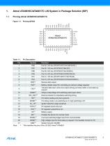
Atmel ATA6616C/ATA6617C LIN System in Package Solution (SIP) NRES WD_OSC Receive data output Battery-related output for controlling an external voltage regulator Transmit data input; active low output (strong pull down) after a local wake-up request (1) Output undervoltage and watchdog reset (open drain) External resistor for adjustable watchdog timing For factory testing only (tie to ground) Ignition detection (edge sensitive) 5V regulator sense input pin For debug mode: Low watchdog is on; high watchdog is off 5V regulator output/driver pin Battery supply Enables the device into normal mode...
Open the catalog to page 3
Table 1-1. Pin Description (Continued) Note:1 This identifies the pins of the LIN SBC Atmel® ATA6624
Open the catalog to page 4
Absolute Maximum Ratings Stresses beyond those listed under “Absolute Maximum Ratings” may cause permanent damage to the device. This is a stress rating only and functional operation of the device at these or any other conditions beyond those indicated in the operational sections of this specification is not implied. Exposure to absolute maximum rating conditions for extended periods may affect device reliability. Parameters ESD according to IBEE LIN EMC Test Spec. 1.0 following IEC 61000-4-2 - Pin VS, LIN, KL_15 (47k/100nF) to GND - Pin WAKE (33 k serial resistor) to GND ESD HBM following STM5.1...
Open the catalog to page 5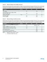
Maximum Ratings of the LIN-SBC (Continued) Stresses beyond those listed under “Absolute Maximum Ratings” may cause permanent damage to the device. This is a stress rating only and functional operation of the device at these or any other conditions beyond those indicated in the operational sections of this specification is not implied. Exposure to absolute maximum rating conditions for extended periods may affect device reliability. Parameters Logic pins (RXD, TXD, EN, NRES, NTRIG, WD_OSC, MODE, TM) Output current NRES PVCC DC voltage VCC DC voltage Table 2-3. Maximum Ratings of the Microcontroller...
Open the catalog to page 6
Master and slave operation possible Supply voltage up to 40V Operating voltage VS = 5V to 27V Typically 10µA supply current during sleep mode Typically 57µA supply current in silent mode Linear Low-drop voltage regulator, 85mA current capability: ● Normal, fail-safe, and silent mode In sleep mode VCC is switched off VCC undervoltage detection (4ms reset time) and watchdog reset logical combined at open drain output NRES Negative trigger input for watchdog Boosting the voltage regulator possible with an external NPN transistor LIN physical layer according to LIN 2.0, 2.1 specification and SAEJ2602-2...
Open the catalog to page 7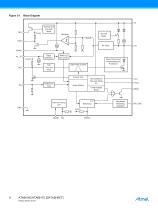
Figure 3-1. Block Diagram VS Normal and Fail-safe Mode Normal Mode Edge Detection Slew Rate Control Control Unit Short Circuit and Overtemperature Protection Debounce Time Normal/Silent/ Fail-safe Mode 5V Undervoltage Reset Mode Select Internal Testing Unit Adjustable Watchdog Oscillator
Open the catalog to page 8
Functional Description Physical Layer Compatibility Since the LIN physical layer is independent from higher LIN layers (e.g., the LIN protocol layer), all nodes with a LIN physical layer according to revision 2.x can be mixed with LIN physical layer nodes, which are according to older versions (i.e., LIN 1.0, LIN 1.1, LIN 1.2, LIN 1.3), without any restrictions. Supply Pin (VS) The LIN operating voltage is VS = 5V to 27V. An undervoltage detection is implemented to disable data transmission if VS falls below VSth < 4V in order to avoid false bus messages. After switching on VS, the IC starts...
Open the catalog to page 9
Output Pin (RXD) The Output pin reports the state of the LIN bus to the microcontroller. LIN high (recessive state) is reported by a high level at RXD; LIN low (dominant state) is reported by a low level at RXD. The output has an internal pull-up resistor with typically 5k to VCC. The AC characteristics can be defined with an external load capacitor of 20pF. The output is short-circuit protected. RXD is switched off in Unpowered Mode (i.e., VS = 0V). 3.3.10 Enable Input Pin (EN) The Enable Input pin controls the operation mode of the device. If EN is high, the circuit is in normal mode with transmission...
Open the catalog to page 10
3.3.18 NTRIG Input Pin The NTRIG Input pin is the trigger input for the window watchdog. A pull-up resistor is implemented. A negative edge triggers the watchdog. The trigger signal (low) must exceed a minimum time ttrigmin to generate a watchdog trigger. 3.3.19 Wake-up Events from Sleep or Silent Mode ● ● ● ● Modes of Operation Figure 3-2. Modes of Operation a: VS > 5V Unpowered Mode VBatt = 0V b: VS < 4V c: Bus wake-up event d: Wake up from WAKE or KL_15 pin Fail-safe Mode VCC: 5V With undervoltage monitoring Communication: OFF Watchdog: ON Silent Mode VCC: 5V With undervoltage monitoring Communication:...
Open the catalog to page 11All Atmel catalogs and technical brochures
 32-bit Microcontrollers
20 Pages
 MCUs Driving Displays
12 Pages
 Touch and 3D Gesture Control
12 Pages
 16-bit MCUs and DSCs
20 Pages
 XLP PIC® MCUs
8 Pages
 8-bit MCUs
16 Pages
 AT93C56B/66B Automotive
17 Pages
 Atmel AT86RF215 Device Family
235 Pages
 AT24C01C/02C
22 Pages
 maXTouch U Series - Flyer
2 Pages


Archived catalogs
 tinyAVR ATtiny24/44/84 Preliminary
240 Pages
 ATmega164P/324P/644P Preliminary
440 Pages
 ATmega48P/88P/168P/328P Preliminary
426 Pages
 ATmega1284P Preliminary
356 Pages
 AT90PWM216/316
359 Pages
 AT90PWM2, AT90PWM3, AT90PWM2B, AT90PWM3B
361 Pages
 ATmega329/3290/649/6490 Preliminary
392 Pages
 ATmega329P/3290P Preliminary
388 Pages
 AT90CAN32/64/128
428 Pages
 AT86RF230 Preliminary
98 Pages
 ATmega48/88/168 Automotive
335 Pages
 ATtiny25, ATtiny45, ATtiny85 Automotive
192 Pages
 ATtiny24/44/84 Automotive Preliminary
225 Pages
 AT86RF231 Preliminary
180 Pages
 Biometrics (Fingerprint Sensor)
20 Pages


- Potentiometer
- Industrial converter
- Ethernet transceiver
- Analog potentiometer
- Low-noise amplifier
- Analog amplifier
- Analog converter
- Circuit board
- Operational amplifier
- 32-bit microcontroller
- Low-power microcontroller
- Analog microcontroller
- High-speed converter
- General purpose microcontroller
- Communication microcontroller
- High-speed amplifier
- Programmable microcontroller
- ARM microcontroller