


ATA5823/ATA5824 UHF Transceiver for ASK and FSK Systems, Full Duplex

ATA5823/ATA5824 UHF Transceiver for ASK and FSK Systems, Full Duplex
- High sensitivity for FSK and ASK at specified data rates and frequencies.
- Low supply current in RX and TX modes.
- Wide data rate support for Manchester FSK and ASK.
- Low IF architecture with high selectivity and blocking capabilities.
- Integrated RX/TX switch and single-ended RF input/output.
- Communication with microcontroller via SPI interface.
- Configurable protocol handling with FIFO-RAM buffering.
- Integrated XTAL capacitors and efficient PA.
- Wide supply voltage range and low power-down current.
- Small QFN48 package.
- Automotive keyless entry and passive entry systems.
- Tire pressure monitoring systems.
- Remote control and alarm systems.
- Energy metering and home automation.
- No need for SAW devices in key fob designs.
- High system integration reduces system cost.
- Single crystal requirement simplifies design.
- Robust design with high isolation and efficient antenna integration.
The Atmel ATA5823/ATA5824 is a UHF ASK/FSK transceiver designed for low power consumption and high integration. It supports multiple data rates and modulation schemes, making it suitable for automotive and remote control applications. The device features a low-IF receiver and a fractional-N synthesizer for FSK transmission, with integrated components to minimize external circuitry.
Pin ConfigurationThe device is housed in a QFN48 package with specific pins for RF input/output, power supply, and microcontroller interface. Key pins include RF_IN, RF_OUT, PWR_H, and various test and control pins.
System Block DiagramThe system block diagram illustrates the integration of signal processing, digital control logic, and RF transceiver components, highlighting the device's capability to handle both RX and TX operations efficiently.
Typical ApplicationsExamples of typical applications include key fob and car systems for bi-directional RKE, utilizing minimal external components for efficient operation at specified frequencies and power levels.
RF Transceiver in Half-duplex ModeThe RF transceiver supports half-duplex operation with a low-IF receiver and a fractional-N synthesizer for efficient signal processing. It offers transparent modes for various coding schemes and ensures robust performance without the need for additional SAW filters in certain applications.
The document discusses the performance characteristics of a receiver operating at 433.92MHz. It highlights a typical image rejection of 30dB and a 3dB system bandwidth of 220kHz. The demodulator requires an 8dB signal-to-noise ratio for 20Kbit/s Manchester encoding with a frequency deviation of ±19.5kHz in FSK mode, resulting in a sensitivity of –105.5dBm.
Input Matching:
Input matching at RF_IN is crucial for achieving high sensitivity. The document provides measured input impedances and suggests matching circuits to align with a 50Ω source impedance. Tables detail the components and their values for optimal matching, with typical sensitivity measurements provided for different bit rates.
Sensitivity Influences:
Sensitivity is affected by frequency offset, temperature, and supply voltage. The document provides data on how these factors influence sensitivity, with a typical range between –102.5dBm and –107dBm. It also discusses the automatic frequency correction feature that enhances system margin.
Frequency Accuracy:
The document outlines the frequency accuracy requirements for crystals used in bi-directional RKE/PEG systems. It specifies tolerances for frequency stability over temperature and aging, emphasizing the need for precise crystal specifications.
RX Supply Current:
Supply current measurements for the receiver in RX mode are provided, showing variations with temperature and supply voltage. This information is critical for applications like key fobs where battery life is a concern.
Blocking and Selectivity:
The receiver's ability to handle large blockers is discussed, with figures illustrating blocking performance at various frequency offsets. The document highlights the receiver's capability to operate without additional SAW filters due to its good intermodulation performance.
Inband Disturbers and Data Processing:
The document describes how the receiver handles inband disturbers, emphasizing the role of the data filter, quasi-peak detector, and data slicer in maintaining performance. It provides carrier-to-noise ratio requirements for different modulation modes.
Test Output:
The document mentions the availability of the internal raw output signal at a specific test pin, useful for diagnostic purposes.
The document outlines the technical specifications and procedures for the ATA5823/ATA5824 transceiver. It includes details on the connection of the drain output to a pull-up resistor for debugging purposes, the RSSI output characteristics, and the frequency synthesizer and channel selection.
RSSI Output:
The RSSI pin provides an analog voltage proportional to the input power level, allowing differentiation of signal strength from various transmitters. The dynamic range is 70dB, with an input power range from –115dBm to –45dBm and a gain of 8mV/dB.
Frequency Synthesizer and Channel Selection:
The synthesizer is a fractional-N design with internal loop filters for both receive and transmit modes. It allows for precise frequency control and modulation, supporting both ASK and FSK transmission. The RF resolution is determined by the XTO frequency divided by 16384.
FSK/ASK Transmission:
The transceiver supports fast modulation capabilities, with FSK modulation deviations of ±18.65kHz for 315MHz and ±19.41kHz for 433.92MHz. The modulation spectrum is clean, meeting ETSI and CEPT regulations.
Output Power Setting and PA Matching:
The Power Amplifier (PA) is designed to deliver consistent current pulses, with output power adjustable via resistor R1. The PA efficiency and output power are influenced by the resistor value and supply voltage. The document provides detailed calculations for optimizing PA efficiency and output power.
Output Power and TX Supply Current:
Output power is affected by supply voltage and temperature, with measurements provided for various conditions. The document highlights the impact of supply voltage on output power variations.
RX/TX Switch:
The RX/TX switch manages the transition between receive and transmit modes, ensuring proper signal routing. The document provides impedance values and guidelines for designing effective RX/TX decoupling.
Matching Networks:
Separate matching networks are described for TX and RX modes, with considerations for impedance matching and minimizing power loss. The document provides component values and configurations for optimal performance.
Tables and Figures:
The document includes several tables and figures illustrating the characteristics and performance of the transceiver, such as RSSI characteristics, output power settings, and matching network configurations.
The document discusses the ATA5823/ATA5824 transceiver, focusing on its RF and oscillator characteristics. It specifies the use of a high Q wire wound inductor with Q > 70 for L2 to minimize RX losses. The impedance at the RF_OUT pin in RX mode is detailed for frequencies 315MHz and 433.92MHz.
Oscillator (XTO):
The XTO is an amplitude regulated Pierce oscillator with integrated load capacitances. It serves as the reference frequency for the fractional-N synthesizer. The document provides formulas for calculating frequency pulling and emphasizes the importance of crystal properties and load capacitances. It also discusses start-up behavior and negative resistance calculations.
Clock and Frequency Control:
The document outlines the relationship between the XTO frequency and RF output frequency, detailing the calculation of the clock frequency (fCLK) and its harmonics. It provides guidance on setting control registers to achieve desired frequencies.
Power Supply:
The transceiver operates within a supply voltage range of 2.15V to 3.6V or 4.4V to 5.25V. It describes the power supply configuration for battery and car applications, including the use of blocking capacitors and voltage regulation.
Operation Modes:
The transceiver has several modes: OFF, IDLE, RX, TX, and FD. The document explains transitions between these modes, power consumption, and reset logic.
Microcontroller Interface:
The interface converts internal digital signals to the microcontroller's voltage level, allowing compatibility with different supply voltages.
Digital Control Logic:
The transceiver's configuration is stored in RAM, accessible via a 4-wire serial interface. The document details the register structure and the default state upon power-up.
- Control Register 1: Configures IRQ pin settings based on the number of bytes in the data buffer and adjusts frequency ranges.
- Control Register 2: Sets operational modes (IDLE, TX, RX) and manages frequency tuning.
- Control Register 3: Adjusts frequency settings further and manages clock output.
- Control Register 4: Configures modulation modes (ASK/FSK) and sleep settings.
- Control Register 5 & 6: Define bit-check parameters and baud rate settings.
- Control Register 7: Manages output levels and transmission bitrate.
- Control Register 8: Adjusts output power settings using an internal resistor.
Exceeding the absolute maximum ratings may cause permanent damage to the device. These ratings are stress limits only, and functional operation at these levels is not guaranteed. Prolonged exposure may affect reliability.
- Junction temperature (Tj): Max 150°C
- Storage temperature (Tstg): Min -55°C, Max +125°C
- Ambient temperature (Tamb): Min -40°C, Max +105°C
- Supply voltages (VS2, VS1, VSINT): Various limits, e.g., VS2 Max +7.2V
- ESD ratings: HBM ±2.5kV, MM ±200V, FCDM ±500V
- Junction to ambient (RthJA): 25 K/W
Parameters are valid for specific temperature and voltage ranges, with typical values given at 3V and 25°C.
- RX_TX_IDLE Mode: Operating frequency range for ATA5824 is 433-435 MHz, and for ATA5823 is 314-316 MHz.
- Supply current in various modes: OFF mode < 10 nA, IDLE mode 260 µA (battery) or 350 µA (car).
- Start-up times: System start-up from OFF to IDLE is 0.3 ms, RX start-up is 1.39 ms, TX start-up is 0.4 ms.
- Supply current: RX mode 10.5 mA, RX polling mode 484 µA.
- Input sensitivity: FSK at 433.92MHz ranges from -103.5 to -107.0 dBm depending on bit rate.
- RSSI output: Dynamic range of 70 dB, with specific levels for 315MHz and 433.92MHz.
- Supply current: TX mode with power amplifier OFF is 6.95 mA.
- Output power: Various configurations provide output power ranging from -2.5 to 11.5 dBm.
- Output power variation: Changes with temperature and supply voltage, e.g., -0.8 to -4.5 dB depending on conditions.
Catalog excerpts

ATA5823/ATA5824 UHF ASK/FSK Transceiver DATASHEET Features ● High FSK sensitivity: –105.5dBm at 20Kbit/s/–109dBm at 2.4Kbit/s (433.92MHz) ● High ASK sensitivity: –111.5dBm at 10Kbit/s/–116dBm at 2.4Kbit/s (100% ASK, carrier level 433.92MHz) ● Low supply current: 10.5mA in RX and TX mode (3V/TX with 5dBm/433.92MHz) ● Data rate 1 to 20Kbit/s Manchester FSK, 1 to 10Kbit/s Manchester ASK ● ASK/FSK receiver uses a low IF architecture with high selectivity, blocking and low intermodulation (typical 3dB blocking 55.5dBC at ±750kHz/60.5dBC at ±1.5MHz and 67dBC at ±10MHz, system I1dBCP = –30dBm/system IIP3 = –20dBm) ● Wide bandwidth AGC to handle large outband blockers above the system I1dBCP ● 226kHz IF (intermediate frequency) with 30dB image rejection and 220kHz system bandwidth to support TPM transmitters using Atmel® ATA5756/ATA5757 transmitters with standard crystals ● Transmitter uses closed loop FSK modulation with fractional-N synthesizer with high PLL bandwidth and an excellent isolation between PLL and PA ● Tolerances of XTAL compensated by fractional-N synthesizer with 800Hz RF resolution ● Integrated RX/TX-switch, single-ended RF input and output ● RSSI (received signal strength indicator) ● Communication to microcontroller with SPI interface working at 500kBit/s maximum ● Configurable self polling and RX/TX protocol handling with FIFO-RAM buffering of received and transmitted data ● 1 push button input and 1 wake-up input are active in power-down mode ● Integrated XTAL capacitors ● PA efficiency: up to 38% (433.92MHz/10dBm/3V) ● Low In-band sensitivity change of typically ±2.0dB within ±75kHz center frequency change in the complete temperature and supply voltage range
Open the catalog to page 1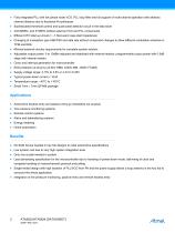
● Fully integrated PLL with low phase noise VCO, PLL loop filter and full support of multi-channel operation with arbitrary channel distance due to fractional-N synthesizer ● Sophisticated threshold control and quasi-peak detector circuit in the data slicer ● 433.92MHz, and 315MHz without external VCO and PLL components ● Efficient XTO start-up circuit (> –1.5kΩ worst case start impedance) ● Changing of modulation type ASK/FSK and data rate without component changes to allow different modulation schemes in TPM and RKE ● Minimal external circuitry requirements for complete system solution ● Adjustable...
Open the catalog to page 2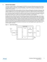
General Description The Atmel® ATA5823/ATA5824 is a highly integrated UHF ASK/FSK multi-channel half-duplex transceiver with low power consumption supplied in a small 7mm × 7mm QFN48 package. The receive part is built as a fully integrated low-IF receiver, whereas direct PLL modulation with the fractional-N synthesizer is used for FSK transmission and switching of the power amplifier for ASK transmission. The device supports data rates of 1Kbit/s to 20Kbit/s (FSK) and 1Kbit/s to 10Kbit/s (ASK) in Manchester, Bi-phase and other codes in transparent mode. The Atmel ATA5824 can be used in the 433MHz...
Open the catalog to page 3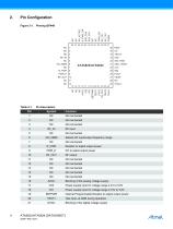
RX_ACTIVE N_PWR_ON DVCC CS_POL Resistor to adjust output power Selects RF input/output frequency range Not connected Pin to select output power Power supply input for voltage range 4.4V to 5.6V Power supply input for voltage range 2.15V to 3.6V Test input, at GND during operation Blocking of the digital voltage supply Blocking of the analog voltage supply Internal Programmable Resistor to adjust output power
Open the catalog to page 4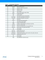
Test input, at GND during operation Reference crystal Reference crystal Microcontroller interface supply voltage Programmable output Interrupt request Clock output to connect a microcontroller Serial data out/transparent mode data out Serial data in/transparent mode data in Serial clock Test output open during operation Chip select for serial interface Switch pin to decouple LNA in TX mode (RKE mode) Output of the RSSI amplifier Capacitor to adjust the lower cut-off frequency data filter Input to switch on the system (active high) Polarity of the serial clock Phase of the serial clock Keyboard...
Open the catalog to page 5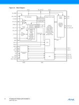
Figure 2-2. Block Diagram AVCC Digital Control Logic Power Supply Frontend Enable RX/TX switch Fractional-N frequency synthesizer Signal Processing (Mixer IF-filter IF-amplifier FSK/ASK Demodulator, Data filter Data Slicer) FREQ FREF TX/RXData buffer Control register Status register Polling circuit Bit-check logic Synchronous logic (Full duplex operation mode) Switches Regulators Wake-up Reset PWR_ON N_PWR_ON Microcontroller interface
Open the catalog to page 6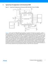
Typical Key Fob Application for Bi-directional RKE Figure 3-1. Typical Key Fob Application for Bi-directional RKE with 5dBm TX Power, 433.92MHz C11 Loop antenna PWR_H SETPWR Figure 3-1 shows a typical 433.92MHz RKE key fob application. The external components are 10 capacitors, 1 resistor, 2 inductors and a crystal. C1 to C3 are 68nF voltage supply blocking capacitors. C5 is a 10nF supply blocking capacitor. C6 is a 15nF fixed capacitor used for the internal quasi-peak detector and for the high-pass frequency of the data filter. C7 to C11 are RF matching capacitors in the range of 1pF to 33pF....
Open the catalog to page 7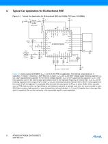
Typical Car Application for Bi-directional RKE Figure 4-1. Typical Car Application for Bi-directional RKE with 10dBm TX Power, 433.92MHz L3 R_PWR PWR_H Figure 4-1 shows a typical 433.92MHz VCC = 4.4V to 5.25V RKE car application. The external components are 11 capacitors, 1 resistor, 4 inductors, a SAW filter and a crystal. C1, C3 and C4 are 68nF voltage supply blocking capacitors. C2 is a 2.2µF supply blocking capacitor for the internal voltage regulator. C5 is a 10nF supply blocking capacitor. C6 is a 15nF fixed capacitor used for the internal quasi-peak detector and for the high-pass frequency...
Open the catalog to page 8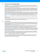
RF Transceiver in Half-duplex Mode According to Figure 2-2 on page 6, the RF transceiver consists of an LNA (Low-Noise Amplifier), PA (Power Amplifier), RX/TX switch, fractional-N frequency synthesizer and the signal processing part with mixer, IF filter, IF amplifier with analog RSSI, FSK/ASK demodulator, data filter and data slicer. In receive mode the LNA pre-amplifies the received signal which is converted down to 226kHz intermediate frequency (IF), filtered and amplified before it is fed into an FSK/ASK demodulator, data filter and data slicer. The RSSI (Received Signal Strength Indicator)...
Open the catalog to page 9All Atmel catalogs and technical brochures
 32-bit Microcontrollers
20 Pages
 MCUs Driving Displays
12 Pages
 Touch and 3D Gesture Control
12 Pages
 16-bit MCUs and DSCs
20 Pages
 XLP PIC® MCUs
8 Pages
 8-bit MCUs
16 Pages
 AT93C56B/66B Automotive
17 Pages
 Atmel AT86RF215 Device Family
235 Pages
 AT24C01C/02C
22 Pages
 maXTouch U Series - Flyer
2 Pages


Archived catalogs
 tinyAVR ATtiny24/44/84 Preliminary
240 Pages
 ATmega164P/324P/644P Preliminary
440 Pages
 ATmega48P/88P/168P/328P Preliminary
426 Pages
 ATmega1284P Preliminary
356 Pages
 AT90PWM216/316
359 Pages
 AT90PWM2, AT90PWM3, AT90PWM2B, AT90PWM3B
361 Pages
 ATmega329/3290/649/6490 Preliminary
392 Pages
 ATmega329P/3290P Preliminary
388 Pages
 AT90CAN32/64/128
428 Pages
 AT86RF230 Preliminary
98 Pages
 ATmega48/88/168 Automotive
335 Pages
 ATtiny25, ATtiny45, ATtiny85 Automotive
192 Pages
 ATtiny24/44/84 Automotive Preliminary
225 Pages
 AT86RF231 Preliminary
180 Pages
 Biometrics (Fingerprint Sensor)
20 Pages


- Potentiometer
- Industrial converter
- Ethernet transceiver
- Analog potentiometer
- Analog amplifier
- Analog converter
- Circuit board
- Operational amplifier
- 32-bit microcontroller
- Low-power microcontroller
- Analog microcontroller
- High-speed converter
- General purpose microcontroller
- Communication microcontroller
- High-speed amplifier
- Programmable microcontroller
- ARM microcontroller