


ATA5428 UHF Transceiver for ASK and FSK Systems, 315 MHz

ATA5428 UHF Transceiver for ASK and FSK Systems, 315 MHz
- Multi-channel half-duplex transceiver with a programmable tuning range of approximately ±2.5MHz.
- High sensitivity for FSK and ASK at specified data rates and frequencies.
- Low supply current in RX and TX modes.
- Data rates supported: 1 to 20Kbit/s for FSK and 1 to 10Kbit/s for ASK.
- Low-IF architecture with high selectivity and blocking capabilities.
- Integrated RX/TX switch and single-ended RF input/output.
- Communication with microcontroller via SPI interface.
- Power management through various operation modes.
- ESD protection and a wide supply voltage range.
- Consumer industrial segment, access control, remote control, alarm systems, energy metering, and home automation.
- High system integration reduces system cost.
- Single crystal requirement simplifies design.
- Efficient power management and protocol handling reduce microcontroller demands.
The Atmel ATA5428 is a highly integrated UHF ASK/FSK transceiver designed for low power consumption and small form factor. It supports multiple frequency bands and data rates, making it suitable for various remote control and access control applications. The device integrates essential components for both base and mobile stations, reducing the need for external components.
Application Circuits- Typical remote control unit applications are detailed for both single and dual battery configurations, highlighting necessary external components like capacitors, resistors, inductors, and crystals.
- Base-station applications are also described, emphasizing the use of SAW filters for high sensitivity and low-pass filters for harmonic suppression.
The RF transceiver includes an LNA, PA, RX/TX switch, fractional-N frequency synthesizer, and signal processing components. It supports both receive and transmit modes with specific modulation techniques for ASK and FSK.
The document discusses the RF resolution, which is determined by the XTO frequency divided by 16384, resulting in specific values at different frequencies (808.9Hz at 433.92MHz and 818.6Hz at 868.3MHz). The frequency control word FREQ can be programmed within a range of 1000 to 6900, allowing for a tuning range of ±2.5MHz within the 433MHz and 868MHz ISM bands.
Procedures:
Care must be taken with harmonics of the CLK output signal to avoid disturbing signal reception. In single-channel systems, using FREQ values between 3803 and 4053 can prevent harmonic interference.
FSK/ASK Transmission:
The document details the modulation capabilities of the synthesizer, allowing for internal FSK modulation with a deviation of ±16.17kHz for 433.92MHz and ±16.37kHz for 868.3MHz. The modulated spectrum is clean, meeting ETSI and CEPT regulations with a simple LC filter.
Output Power Setting and PA Matching:
The Power Amplifier (PA) is described as a single-ended open collector stage with a reference current controlled by resistor R1. The output power range can be adjusted between 0dBm to 10dBm depending on the PWR_H pin setting. The document provides detailed calculations for current consumption and PA efficiency.
Output Power and TX Supply Current:
Tables provide measurements of output power and supply current at different temperatures and supply voltages, highlighting the impact of supply voltage on output power variations.
RX/TX Switch:
The RX/TX switch decouples the LNA from the PA in TX mode and directs received power to the LNA in RX mode. The document provides an equivalent circuit and discusses the impedance characteristics.
Matching Network:
In TX mode, the document describes the matching network configuration, including the use of a transmission line and capacitors to achieve a parallel resonant high impedance circuit. In RX mode, the impedance characteristics and matching considerations are detailed.
XTO:
The XTO is an amplitude-regulated Pierce oscillator with integrated load capacitances. The document discusses the frequency accuracy and compensation for frequency errors, as well as the impact of temperature and supply voltage on the XTO frequency.
The document discusses the ATA5428 transceiver, focusing on its crystal oscillator (XTO) characteristics. The XTO has a negative resistance of about 2kΩ, with worst-case scenarios maintaining resistance above 1.5kΩ. Recommended crystal parameters include Cm = 3.0fF to 7.0fF, CLN = 9pF, Rm < 120Ω, and C0 = 1.0pF to 2.2pF. The start-up time is influenced by the time constant τ, and the oscillation amplitude is detected after 10τ to 20τ.
Procedures:
The document outlines procedures for setting control registers to achieve desired frequencies. The relationship between fXTO and fRF is crucial, with specific values provided for different frequency settings. The CLK output harmonics must be managed to avoid interference with RF signals.
Power Supply:
The ATA5428 operates within a supply voltage range of 2.4V to 3.6V or 4.4V to 6.6V. Various pins (VS1, VS2, VAUX, VSINT) are used for different voltage inputs, with specific configurations for 1 Li battery (3V) and 2 Li battery (6V) applications. Voltage regulators ensure stable operation, and power modes (OFF, AUX, IDLE) are described with their transitions and conditions.
Microcontroller Interface:
The interface converts internal digital signals to the microcontroller's voltage level, allowing flexible power supply configurations.
Digital Control Logic:
The transceiver's configuration is stored in RAM, accessible via a 4-wire serial interface. The RAM includes a data buffer and control registers, while the status register is separately readable.
Recommendations:
To minimize current consumption, load capacitors are partially switched off in IDLE and Sleep modes. Careful layout of the CLK signal on the PCB is advised to prevent interference in multichannel systems.
- Control Register 1: Configures IRQ pin behavior based on data buffer status and errors in RX and TX modes. It also sets operational modes like IDLE, TX, and RX.
- Control Register 2: Manages frequency settings and modulation modes, including Manchester and NRZ modes.
- Control Register 3: Controls output voltage supply and clock output, with settings for frequency tuning.
- Control Register 4: Configures sleep modes and extended sleep settings.
- Control Register 5: Sets bit-check parameters and minimum limit settings for RX and TX modes.
- Control Register 6: Defines baud rate ranges and maximum limit settings.
- Pin Tn: Used to switch the transceiver from OFF to IDLE mode, with debounce logic to handle events.
- Pin PWR_ON: Activates the transceiver from OFF to IDLE mode, setting power and clock outputs.
- Low Battery Indicator: Monitors VSOUT voltage, setting a status bit if it drops below 2.38V.
- Pin VAUX: Switches the transceiver to AUX mode when voltage exceeds 3.5V, with status indication.
- Write TX/RX Data Buffer: Allows successive writing of bytes into the TX/RX data buffer during a TX operation. An echo of the command and TX data bytes is provided on the SDO_TMDO pin.
- Read Control/Status Register: Control and status registers can be read individually or successively.
- Write Control Register: Control registers can be written individually or successively, with an echo provided on the SDO_TMDO pin.
- OFF Command: Sets the transceiver to OFF mode under specific conditions involving AVCC_EN, PWR_ON, and key inputs.
- Delete IRQ: Sets the IRQ pin to low.
The command structure uses the three most significant bits to indicate the command type, while bits 0 to 4 describe the target address for control or status registers.
4-wire Serial Interface
The interface includes Chip Select (CS), Serial Clock (SCK), Serial Data Input (SDI_TMDI), and Serial Data Output (SDO_TMDO). Data is synchronized with the serial clock.
Operation Modes
- RX Operation: The transceiver consumes less than 1mA in RX operation, using a polling circuit to periodically enable the signal path and verify the presence of a valid transmitter signal.
- RX Polling Mode: Involves a cycle of sleep, start-up, and bit-check modes to manage power consumption and signal verification.
- Sleep Mode: Defined by control register settings, with a maximum sleep period of about 38ms or 300ms depending on configuration.
- Start-up Mode: Involves enabling and stabilizing the PLL and signal processing circuits.
- Bit-check Mode: Examines incoming data to distinguish valid signals from noise, using programmable time windows for edge-to-edge tests.
The bit-check configuration allows setting the number of bits to be checked, affecting the likelihood of switching to receiving mode and the time taken for bit-checks.
The document outlines the programming of bit-check limits using formulas involving Lim_min and Lim_max, which are defined in control registers 5 and 6. The timing diagrams (Figures 9-5 to 9-7) illustrate scenarios where the bit-check counter value CV_Lim is within or outside these limits. The bit-check process is statistical, with TBit-check varying based on bit-rate range and TXDCLK.
Upon successful bit checks, the transceiver enters receiving mode, activating a connected microcontroller. Data is buffered and checked against time frame limits. Errors trigger interrupts and reset the transceiver to start-up mode. The document details the handling of data streams and buffer management to prevent overflow.
For maximum sensitivity, specific Lim_min and Lim_max values are recommended, with a minimum of 6 bits checked to avoid frequent wake-ups due to noise.
The transceiver is set to TX mode via control register 1. TX parameters must be configured before activation. The document describes the process of loading and transmitting data, with emphasis on preventing buffer overflow. Transparent mode is also discussed, where the TX/RX data buffer is bypassed.
Interrupts signal various operating conditions to a microcontroller. The document advises immediate deletion of interrupts to prevent loss of subsequent signals. Specific conditions and actions for handling interrupts during TX and RX operations are detailed.
This section outlines the stress limits for the ATA5428 device, beyond which permanent damage may occur. Key parameters include junction temperature (up to 150°C), storage temperature (-55°C to +125°C), and various supply voltages with specific maximum values. ESD ratings are also provided for different models.
Thermal Resistance
The thermal resistance from junction to ambient is specified as 25 K/W.
Electrical Characteristics: General
The device is manufactured for industrial use and is not recommended for automotive applications. Parameters are specified for different applications (1-battery, 2-battery, and base-station) with typical values at 433.92 MHz. Key characteristics include supply current in various modes, system start-up times, and input sensitivity for FSK and ASK modes.
Receiver/RX Mode
Details on supply current in RX mode, input sensitivity for FSK and ASK, and maximum frequency offset in FSK mode are provided. The section also covers system noise figure, intermediate frequency, and system bandwidth.
Power Amplifier/TX Mode
This section specifies supply current and output power for different TX modes, including power amplifier ON and OFF states. It also covers output power variation across temperature and supply voltage ranges.
XTO (Crystal Oscillator)
Information on XTO pulling due to tolerances, transconductance at start, and start-up time is provided. Maximum C0 of XTAL required for stable operation is also mentioned.
- General Description: Provides an overview of the ATA5428 RF Transceiver, highlighting its capabilities and intended use cases.
- Application Circuits: Describes typical applications for the transceiver, including remote control units and base-station applications with various power supply configurations.
- RF Transceiver: Details the technical specifications of the RF transceiver, including receiver sensitivity, frequency accuracy, and power settings.
- Power Supply: Discusses different power modes and configurations, including applications with 1 or 2 lithium batteries.
- Microcontroller Interface: Outlines the interface between the transceiver and a microcontroller, including digital control logic and register structures.
- Transceiver Configuration: Provides command structures for configuring the transceiver, including reading and writing data buffers and control registers.
- Operation Modes: Describes the various operation modes of the transceiver, including RX and TX operations and interrupt handling.
- Electrical Characteristics: Lists the electrical specifications for different applications, including battery and base-station configurations.
- Ordering Information: Updated section providing details on how to order the transceiver.
- Revision History: Documents changes made in each revision, including template updates and part deletions.
Catalog excerpts
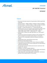
ATA5428 UHF ASK/FSK Transceiver DATASHEET Features ● Multi channel half-duplex transceiver with approximately ±2.5MHz programmable tuning range ● High FSK sensitivity: –106dBm at 20Kbit/s/–109.5dBm at 2.4Kbit/s (433.92MHz) ● High ASK sensitivity: –112.5dBm at 10Kbit/s/–116.5dBm at 2.4Kbit/s (433.92MHz) ● Low supply current: 10.5mA in RX and TX Mode (3V/TX with 5dBm) ● Data Rate: 1 to 20Kbit/s Manchester FSK, 1 to 10Kbit/s Manchester ASK ● ASK/FSK receiver uses a low-IF architecture with high selectivity, blocking, and low intermodulation (typical blocking 55dB at ±750kHz/61dB at ±1.5MHz and 70dB at ±10MHz, system I1dBCP = –30dBm/system IIP3 = –20dBm) ● 226kHz/237kHz IF frequency with 30dB image rejection and 170kHz usable IF bandwidth ● Transmitter uses closed loop fractional-N synthesizer for FSK modulation with a high PLL bandwidth and an excellent isolation between PLL/VCO and PA ● Tolerances of XTAL compensated by fractional-N synthesizer with 800Hz RF resolution ● Integrated RX/TX-switch, single-ended RF input and output ● RSSI (Received Signal Strength Indicator) ● Communication to microcontroller with SPI interface working at max.500kBit/s ● Configurable self polling and RX/TX protocol handling with FIFO-RAM buffering of received and transmitted data ● Five push button inputs and one wake-up input are active in power-down mode ● integrated XTAL capacitors ● PA efficiency: up to 38% (433.92MHz/10dBm/3V) ● Low in-band sensitivity change of typically ±1.8dB within ±58kHz center frequency change in the complete temperature and supply voltage range ● Supply voltage switch, supply voltage regulator, reset generation, clock/interrupt generation and low battery indicator for microcontroller
Open the catalog to page 1
● Fully integrated PLL with low phase noise VCO, PLL loop filter and full support of multi-channel operation with arbitrary channel distance due to fractional-N synthesizer ● Sophisticated threshold control and quasi-peak detector circuit in the data slicer ● Power management via different operation modes ● 433.92MHz and 868.3MHz without external VCO and PLL components ● Inductive supply with voltage regulator if battery is empty (AUX mode) ● Efficient XTO start-up circuit (> –1.5kΩ worst case real start-up impedance) ● Changing of modulation type ASK/FSK and data rate without component changes...
Open the catalog to page 2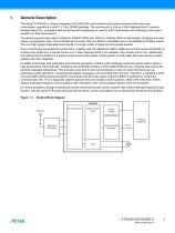
General Description The Atmel® ATA5428 is a highly integrated UHF ASK/FSK multi-channel half-duplex transceiver with low power consumption supplied in a small 7 x 7mm QFN48 package. The receive part is built as a fully integrated low-IF receiver, whereas direct PLL modulation with the fractional-N synthesizer is used for FSK transmission and switching of the power amplifier for ASK transmission. The device supports data rates of 1Kbit/s to 20Kbit/s (FSK) and 1Kbit/s to 10Kbit/s (ASK) in Manchester, Bi-phase and other codes in transparent mode. The ATA5428 can be used in the 431.5MHz to 436.5MHz...
Open the catalog to page 3
Symbol Function 433_N868 Selects RF input/output frequency range R_PWR Resistor to adjust output power PWR_H Pin to select output power AVCC Blocking of the analog voltage supply VS2 Power supply input for voltage range 4.4V to 6.6V VS1 Power supply input for voltage range 2.4V to 3.6V VAUX Auxiliary supply voltage input
Open the catalog to page 4
Test input, at GND during operation Blocking of the digital voltage supply Output voltage power supply for external devices Test input, at GND during operation Reference crystal Reference crystal Interrupt request Clock output to connect a microcontroller Serial data out/transparent mode data out Switch pin to decouple LNA in TX mode Key input 5 (can also be used to switch on the system (active low)) Key input 4 (can also be used to switch on the system (active low)) Key input 3 (can also be used to switch on the system (active low)) Key input 2 (can also be used to switch on the system (active...
Open the catalog to page 5
Figure 1-3. Block Diagram AVCC Digital Control Logic Power Supply Frontend Enable RX/TX Switch TX_DATA (FSK) Switches Regulators Wake-up Reset Fractional-N Frequency Synthesizer Signal Processing (Mixer IF Filter IF Amplifier FSK/ASK Demodulator, Data Filter Data Slicer) TX/RX - Data Buffer Control Register Status Register Polling Circuit Bit-check Logic Microcontroller Interface SDI_TMDI SDO_TMDO
Open the catalog to page 6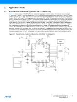
Application Circuits Typical Remote Control Unit Application with 1 Li Battery (3V) Figure 2-1 shows a typical 433.92MHz Remote Control Unit application with one battery. The external components are 11 capacitors, 1 resistor, 2 inductors and a crystal. C1 to C4 are 68nF voltage supply blocking capacitors. C5 is a 10nF supply blocking capacitor. C6 is a 15nF fixed capacitor used for the internal quasi-peak detector and for the high-pass frequency of the data filter. C7 to C11 are RF matching capacitors in the range of 1pF to 33pF. L1 is a matching inductor of about 5.6nH to 56nH. L2 is a feed...
Open the catalog to page 7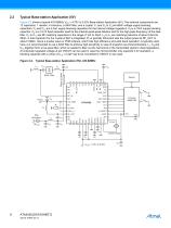
Typical Base-station Application (5V) Figure 2.2 shows a typical 433.92MHz VCC = 4.75V to 5.25V Base-station Application (5V). The external components are 12 capacitors, 1 resistor, 4 inductors, a SAW filter, and a crystal. C1 and C3 to C4 are 68nF voltage supply blocking capacitors. C2 and C12 are 2.2µF supply blocking capacitors for the internal voltage regulators. C5 is a 10nF supply blocking capacitor. C6 is a 15 nF fixed capacitor used for the internal quasi-peak detector and for the high-pass frequency of the data filter. C7 to C11 are RF matching capacitors in the range of 1pF to 33pF....
Open the catalog to page 8
Typical Remote Control Unit Application, 2 Li Batteries (6V) Figure 2-3 shows a typical 433.92Hz 2 Li battery Remote Control Unit application. The external components are 11 capacitors, 1 resistor, 2 inductors and a crystal. C1 and C4 are 68nF voltage supply blocking capacitors. C2 and C3 are 2.2µF supply blocking capacitors for the internal voltage regulators. C5 is a 10nF supply blocking capacitor. C6 is a 15nF fixed capacitor used for the internal quasi-peak detector and for the high-pass frequency of the data filter. C7 to C11 are RF matching capacitors in the range of 1pF to 33pF. L1 is...
Open the catalog to page 9All Atmel catalogs and technical brochures
 32-bit Microcontrollers
20 Pages
 MCUs Driving Displays
12 Pages
 Touch and 3D Gesture Control
12 Pages
 16-bit MCUs and DSCs
20 Pages
 XLP PIC® MCUs
8 Pages
 8-bit MCUs
16 Pages
 AT93C56B/66B Automotive
17 Pages
 Atmel AT86RF215 Device Family
235 Pages
 AT24C01C/02C
22 Pages
 maXTouch U Series - Flyer
2 Pages


Archived catalogs
 tinyAVR ATtiny24/44/84 Preliminary
240 Pages
 ATmega164P/324P/644P Preliminary
440 Pages
 ATmega48P/88P/168P/328P Preliminary
426 Pages
 ATmega1284P Preliminary
356 Pages
 AT90PWM216/316
359 Pages
 AT90PWM2, AT90PWM3, AT90PWM2B, AT90PWM3B
361 Pages
 ATmega329/3290/649/6490 Preliminary
392 Pages
 ATmega329P/3290P Preliminary
388 Pages
 AT90CAN32/64/128
428 Pages
 AT86RF230 Preliminary
98 Pages
 ATmega48/88/168 Automotive
335 Pages
 ATtiny25, ATtiny45, ATtiny85 Automotive
192 Pages
 ATtiny24/44/84 Automotive Preliminary
225 Pages
 AT86RF231 Preliminary
180 Pages
 Biometrics (Fingerprint Sensor)
20 Pages


- Potentiometer
- Industrial converter
- Ethernet transceiver
- Analog potentiometer
- Low-noise amplifier
- Analog amplifier
- Analog converter
- Circuit board
- Operational amplifier
- 32-bit microcontroller
- Low-power microcontroller
- Analog microcontroller
- High-speed converter
- General purpose microcontroller
- Communication microcontroller
- High-speed amplifier
- Programmable microcontroller
- ARM microcontroller