ATA2526 IR Receiver IC Optimized for Standard Remote Control Solutions, Supply Voltage 3 - 5V
1 /13Pages

ATA2526 IR Receiver IC Optimized for Standard Remote Control Solutions, Supply Voltage 3 - 5V
1 /13Pages
Catalog excerpts

ATA2526 Low-voltage IR Receiver ASSP DATASHEET Features ● No external components except PIN diode ● Supply-voltage range: 2.7V to 5.5V ● High sensitivity due to automatic sensitivity adaption (AGC) and automatic strong signal adaption (ATC) ● Automatic supply voltage adaptation ● High immunity against disturbances from daylight and lamps ● Small size and innovative pad layout ● Available for carrier frequencies between 33kHz to 40kHz and 56kHz; adjusted by zener diode fusing ±2.5% ● TTL and CMOS compatible Applications ● Home entertainment applications ● Home appliances ● Remote control equipment
Open the catalog to page 1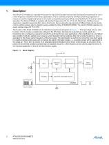
Description The Atmel® IC ATA2526 is a complete IR receiver for data communication that has been developed and optimized for use in carrier-frequency-modulated transmission applications. The IC combines small size with high sensitivity suppression of noise as caused by daylight and lamps. An innovative and patented pad layout offers unique flexibility for IR receiver module assembly. The Atmel ATA2526 is available with standard frequencies (33, 36, 37, 38, 40, 56kHz) and 3 different noise suppression regulation types (standard, lamp, short burst), thus covering the requirements of different high-volume...
Open the catalog to page 2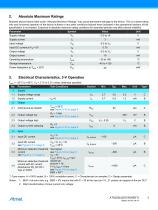
2. Absolute Maximum Ratings Stresses beyond those listed under "Absolute Maximum Ratings" may cause permanent damage to the device. This is a stress rating only and functional operation of the device at these or any other conditions beyond those indicated in the operational sections of this specification is not implied. Exposure to absolute maximum rating conditions for extended periods may affect device reliability. Operating temperature Tamb -25 to +85 °C Storage temperature Tstg -40 to+125 °C Power dissipation at Tamb = 25°C Ptot 30 mW 3. Electrical Characteristics, 3-V Operation Tamb = -25°C...
Open the catalog to page 3
Electrical Characteristics, 3-V Operation (Continued) Tamb = –25°C to +85°C, VS = 2.7V to 3.3V unless otherwise specified. No. Test signal: see Figure 5-9 on page 9 VS = 3V, Tamb = 25°C Maximum detection threshold IIN_DC = 1µA current with square pp VIN > 0V burst N = 16 f = f0; tPER = 10ms see Figure 5-8 on page 8 BER = 5%(1) Test Conditions Controlled Amplifier and Filter Maximum value of variable gain (CGA) Minimum value of variable gain (CGA) Center frequency fusing accuracy of bandpass Overall accuracy center frequency of bandpass Overall accuracy center frequency of bandpass *) Type means:...
Open the catalog to page 4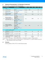
Electrical Characteristics, 5-V Operation (Continued) Tamb = –25°C to +85°C, VS = 4.5V to 5.5V unless otherwise specified. No. 7 Test Conditions Input DC current see Figure 5-4 on page 7 Minimum detection threshold current see Figure 5-2 on page 6 Test signal: see Figure 5-9 on page 9 VS = 5V Tamb = 25°C IIN_DC = 1µA Minimum detection square pp threshold current with AC burst N = 16 current disturbance f = f0; tPER = 10ms IIN_AC100 = 3µA at 100Hz see Figure 5-8 on page 8 BER = 50(1) Maximum detection threshold current with VIN > 0V Test signal: see Figure 5-9 on page 9 VS = 5V, Tamb = 25°C IIN_DC...
Open the catalog to page 5
Typical Electrical Curves at Tamb = 25°C Figure 5-1. IEemin versus IIN_DC, VS = 3V 100 VS = 3V Figure 5-2. IEemin versus IIN_DC, VS = 5V 100 VS = 5V Figure 5-3. VIN versus IIN_DC, VS = 3V 3.5 VS = 3V
Open the catalog to page 6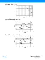
Figure 5-4. VIN versus IIN_DC, VS = 5V 3.5 VS = 5V Figure 5-5. Data Transmission Rate, VS = 3V 4000 3500 3060 Short burst type Standard type Lamp type Figure 5-6. Data Transmission Rate, VS = 5V 4000 3415 3500 Short burst type Lamp type
Open the catalog to page 7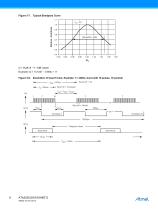
Figure 5-7. Typical Bandpass Curve 1.1 VS = 3V Relative Amplitude Q = f/f0/B; B → –3dB values Example: Q = 1/(1.047 – 0.954) = 11 Figure 5-8. Illustration of Used Terms, Example: f = 33kHz, burst with 16 pulses, 16 periods Period (P = 16) tPER = 970µs Burst (N = 16 pulses) tGAP > tDON + tDOFF OUT Telegram Pause Data Word Data Word
Open the catalog to page 8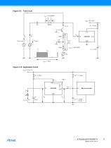
Figure 5-9. Test Circuit IEe = ΔU1/400kΩ ΔU1 Figure 5-10. Application Circuit VDD = 3V to 5V
Open the catalog to page 9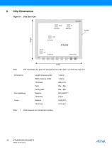
Chip Dimensions Figure 6-1. Chip Size in µm 1080,960 GND 393,839 width Note: Pad coordinates are given for lower left corner of the pad in µm from the origin 0,0 Length inclusive scribe Width inclusive scribe Fusing pads Value depends on manufacture location.
Open the catalog to page 10
Delivery: unsawn wafers (DDW) in box
Open the catalog to page 11
Revision History Please note that the following page numbers referred to in this section refer to the specific revision mentioned, not to this document. Revision No. • Put datasheet in the latest template • Thermal Resistance table deleted • Pin columns in Electrical Characteristics tables deleted • Put datasheet in newest template • Section 8 “Ordering Information” on page 12 changed • Features on page 1 changed • Applications on page 1 changed • Section 1 “Description” on page 1 changed • Section 2 “Pin Configuration” on page 2 changed • Number 2.2, 3.3 and 3.4 of Section 5 “Electrical Characteristics,...
Open the catalog to page 12
XXXXXX Atmel Corporation 1600 Technology Drive, San Jose, CA 95110 USA © 2014 Atmel Corporation. / Rev.: Rev.: 4905G–AUTO–04/14 Atmel®, Atmel logo and combinations thereof, Enabling Unlimited Possibilities®, and others are registered trademarks or trademarks of Atmel Corporation or its subsidiaries. Other terms and product names may be trademarks of others. DISCLAIMER: The information in this document is provided in connection with Atmel products. No license, express or implied, by estoppel or otherwise, to any intellectual property right is granted by this document or in connection with the...
Open the catalog to page 13All Atmel catalogs and technical brochures
 32-bit Microcontrollers
20 Pages
 MCUs Driving Displays
12 Pages
 Touch and 3D Gesture Control
12 Pages
 16-bit MCUs and DSCs
20 Pages
 XLP PIC® MCUs
8 Pages
 8-bit MCUs
16 Pages
 AT93C56B/66B Automotive
17 Pages
 Atmel AT86RF215 Device Family
235 Pages
 AT24C01C/02C
22 Pages
 maXTouch U Series - Flyer
2 Pages


Archived catalogs
 tinyAVR ATtiny24/44/84 Preliminary
240 Pages
 ATmega164P/324P/644P Preliminary
440 Pages
 ATmega48P/88P/168P/328P Preliminary
426 Pages
 ATmega1284P Preliminary
356 Pages
 AT90PWM216/316
359 Pages
 AT90PWM2, AT90PWM3, AT90PWM2B, AT90PWM3B
361 Pages
 ATmega329/3290/649/6490 Preliminary
392 Pages
 ATmega329P/3290P Preliminary
388 Pages
 AT90CAN32/64/128
428 Pages
 AT86RF230 Preliminary
98 Pages
 ATmega48/88/168 Automotive
335 Pages
 ATtiny25, ATtiny45, ATtiny85 Automotive
192 Pages
 ATtiny24/44/84 Automotive Preliminary
225 Pages
 AT86RF231 Preliminary
180 Pages
 Biometrics (Fingerprint Sensor)
20 Pages


- Transceiver module
- Potentiometer
- Industrial converter
- Ethernet transceiver
- Analog potentiometer
- Low-noise amplifier
- Microcontroller
- Analog amplifier
- Analog converter
- Circuit board
- Operational amplifier
- 32-bit microcontroller
- Low-power microcontroller
- Analog microcontroller
- High-speed converter
- General purpose microcontroller
- DAC converter
- Communication microcontroller
- High-speed amplifier
- ARM microcontroller