AT93C56B/66B Automotive
1 /17Pages

AT93C56B/66B Automotive
1 /17Pages
Catalog excerpts

Features • Medium-voltage and Standard-voltage Operation - VCC = 2.5V to 5.5V • Automotive Temperature Range -40°C to 125°C • User-selectable Internal Organization - 2K: 256 x 8 or 128 x 16 - 4K: 512 x 8 or 256 x 16 • 3-wire Serial Interface • Sequential Read Operation • 2MHz Clock Rate • Self-timed Write Cycle (5ms max) • High Reliability - Endurance: 1,000,000 Write Cycles - Data Retention: 100 Years • Lead-free/Halogen-free Devices Available • 8-lead JEDEC SOIC and 8-lead TSSOP Packages Description The Atmel® AT93C56B/66B provides 2,048/4,096 bits of Serial Electrically Erasable Programmable Read-Only Memory (EEPROM). The EEPROM is organized as 128/256 words of 16 bits each when the ORG pin is connected to VCC and 256/512 words of 8 bits each when it is tied to ground. The device is optimized for use in many automotive applications where low-power and low-voltage operations are essential. AT93C56B/66B is available in space-saving 8-lead JEDEC SOIC and 8-lead TSSOP packages. AT93C56B/66B is enabled through the Chip Select (CS) pin and accessed via a 3-wire serial interface consisting of Data Input (DI), Data Output (DO), and Shift Clock (SK). Upon receiving a Read instruction at DI, the address is decoded and the data is clocked out serially on the data output pin DO. The write cycle is completely self-timed and no separate erase cycle is required before write. The write cycle is only enabled when the part is in the Erase/Write Enable state. When CS is brought high following the initiation of a write cycle, the DO pin outputs the Ready/Busy status of the part. AT93C56B/66B operates from 2.5V to 5.5V.
Open the catalog to page 1
Pin Configuration and Pinouts Figure 1. Pin Configurations (Top View) (Top View) Note: Drawings are not to scale. and functional operation of the device at these or Voltage on any pin any other conditions beyond those indicated in
Open the catalog to page 2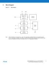
Block Diagram Figure 3-1. Block Diagram Address Decoder Data Register Output Buffer Mode Decode Logic Clock Generator When the ORG pin is connected to VCC, the “x 16” organization is selected. When it is connected to ground, the “x 8” organization is selected. If the ORG pin is left unconnected and the application does not load the input beyond the capability of the internal 1m pullup, then the “x 16” organization is selected.
Open the catalog to page 3
4. Electrical Characteristics4.1 Pin Capacitance Table 4-1. Pin Capacitance(1) Applicable over recommended operating range from TA = 25°C, f = 1.0MHz, VCC = +5.0V (unless otherwise noted). Note: 1. VIL min and VIH max are reference only and are not tested.
Open the catalog to page 4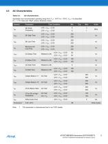
Applicable over recommended operating range from TA = 40°C to + 125°C, VCC = As Specified, CL = 1 TTL Gate and 100pF (unless otherwise noted). Symbol Write Cycle Time Test Condition
Open the catalog to page 5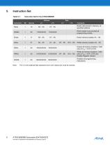
Note: The X in the address field represent don’t care values and must be clocked.
Open the catalog to page 6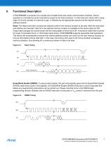
Functional Description AT93C56B/66B is accessed via a simple and versatile three-wire serial communication interface. Device operation is controlled by seven instructions issued by the host processor. A valid instruction starts with a rising edge of CS and consists of a start bit (Logic 1) followed by the appropriate opcode and the desired memory address location. Read: The Read instruction contains the address code for the memory location to be read. After the instruction and address are decoded, data from the selected memory location is available at the serial output pin DO. Output data changes...
Open the catalog to page 7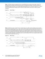
Erase: The Erase instruction programs all bits in the specified memory location to the Logical 1 state. The self-timed erase cycle starts once the Erase instruction and address are decoded. The DO pin outputs the Ready/Busy status of the part if CS is brought high after being kept low for a minimum of 250ns (tCS). A Logic 1 at pin DO indicates that the selected memory location has been erased, and the part is ready for another instruction. Figure 6-3. CHECK STATUS High Impedance High Impedance BUSY READY Write: The Write instruction contains the 8 or 16 bits of data to be written into the specified...
Open the catalog to page 8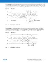
Erase All (ERAL): The Erase All (ERAL) instruction programs every bit in the memory array to the Logic 1 state and is primarily used for testing purposes. The DO pin outputs the ready/busy status of the part if CS is brought high after being kept low for a minimum of 250ns (tCS). The ERAL instruction is valid only at VCC = 5.0V 10%. Figure 6-5. CHECK STATUS High Impedance High Impedance READY Write All (WRAL): The Write All (WRAL) instruction programs all memory locations with the data patterns specified in the instruction. The DO pin outputs the Ready/Busy status of the part if CS is brought...
Open the catalog to page 9
Erase/Write Disable (EWDS): To protect against accidental data disturb, the Erase/Write Disable (EWDS) instruction disables all programming modes and should be executed after all programming operations. The operation of the Read instruction is independent of both the EWEN and EWDS instructions and can be executed at any time.
Open the catalog to page 10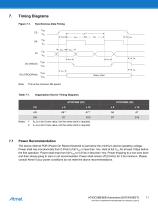
Figure 7-1. Synchronous Data Timing Note: This is the minimum SK period. Table 7-1. Organization Key for Timing Diagrams Notes: 1. A8 is a don’t care value, but the extra clock is required. 2. A7 is a don’t care value, but the extra clock is required. 7.1 Power Recommendation The device internal POR (Power-On Reset) threshold is just below the minimum device operating voltage. Power shall rise monotonically from 0.0Vdc to full VCC in less than 1ms. Hold at full VCC for at least 100^s before the first operation. Power shall drop from full VCC to 0.0Vdc in less than 1ms. Power dropping to a...
Open the catalog to page 11
Shipping Carrier Option T = Tape and Reel Operating Voltage D = 2.5V to 5.5V Package Device Grade P = Lead-free / Halogen-free AutomotiveTemperature Range (-40°C to +125°C) Package Type SS = JEDEC SOIC X = TSSOP
Open the catalog to page 12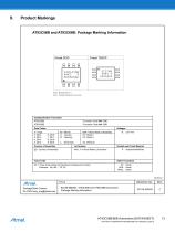
AT93C56B and AT93C66B: Package Marking Information Note 1: O designates pin 1 Note 2: Package drawings are not to scale Package Mark Contact' 93C56-66BAM, AT93C56B and AT93C66B Automotive [email protected] Package Marking |nformation
Open the catalog to page 13All Atmel catalogs and technical brochures
 32-bit Microcontrollers
20 Pages
 MCUs Driving Displays
12 Pages
 Touch and 3D Gesture Control
12 Pages
 16-bit MCUs and DSCs
20 Pages
 XLP PIC® MCUs
8 Pages
 8-bit MCUs
16 Pages
 Atmel AT86RF215 Device Family
235 Pages
 AT24C01C/02C
22 Pages
 maXTouch U Series - Flyer
2 Pages


Archived catalogs
 tinyAVR ATtiny24/44/84 Preliminary
240 Pages
 ATmega164P/324P/644P Preliminary
440 Pages
 ATmega48P/88P/168P/328P Preliminary
426 Pages
 ATmega1284P Preliminary
356 Pages
 AT90PWM216/316
359 Pages
 AT90PWM2, AT90PWM3, AT90PWM2B, AT90PWM3B
361 Pages
 ATmega329/3290/649/6490 Preliminary
392 Pages
 ATmega329P/3290P Preliminary
388 Pages
 AT90CAN32/64/128
428 Pages
 AT86RF230 Preliminary
98 Pages
 ATmega48/88/168 Automotive
335 Pages
 ATtiny25, ATtiny45, ATtiny85 Automotive
192 Pages
 ATtiny24/44/84 Automotive Preliminary
225 Pages
 AT86RF231 Preliminary
180 Pages
 Biometrics (Fingerprint Sensor)
20 Pages


- Transceiver module
- Potentiometer
- Industrial converter
- Ethernet transceiver
- Analog potentiometer
- Low-noise amplifier
- Microcontroller
- Analog amplifier
- Analog converter
- Circuit board
- Operational amplifier
- 32-bit microcontroller
- Low-power microcontroller
- Analog microcontroller
- High-speed converter
- General purpose microcontroller
- DAC converter
- Communication microcontroller
- High-speed amplifier
- ARM microcontroller