AT93C46E 1Kb, 3-Wire Bus Serial EEPROM supports x16 data format memory organization.
1 /18Pages

AT93C46E 1Kb, 3-Wire Bus Serial EEPROM supports x16 data format memory organization.
1 /18Pages
Catalog excerpts

AT93C46E 3-wire Serial EEPROM 1K (64 x 16) DATASHEET Features Low-voltage and Standard-voltage Operation ̶ User-selectable Internal Organization 3-wire Serial Interface 2MHz Clock Rate (5.0V) Self-timed Write Cycle (5ms Max) High Reliability Endurance: 1,000,000 Write Cycles Data Retention: 100 Years 8-lead PDIP, 8-lead JEDEC SOIC, 8-lead, and TSSOP Packages Lead-free/Halogen-free Device Description The Atmel® AT93C46E provides 1,024 bits of Serial Electrically-Erasable Programmable Read-Only Memory (EEPROM) organized as 64 words of 16 bits each. The device is optimized for use in many industrial and commercial applications where low-power and low-voltage operation are essential. The AT93C46E is available in space-saving 8-lead PDIP, 8-lead JEDEC SOIC, 8-lead, and TSSOP packages. The AT93C46E is enabled through the Chip Select pin (CS) and accessed via a 3-wire serial interface consisting of Data Input (DI), Data Output (DO), and Shift Clock (SK). Upon receiving a Read instruction at DI, the address is decoded and the data is clocked out serially on the data output DO pin. The write cycle is completely self-timed, and no separate erase cycle is required before write. The write cycle is only enabled when the part is in the Erase/Write Enable state. When CS is brought high following the initiation of a write cycle, the DO pin outputs the Ready/Busy status of the part. The AT93C46E is available from 1.8V to 5.5V.
Open the catalog to page 1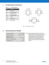
Pin Descriptions and Pinouts Table 1-1. Function Chip Select Serial Data Output Power Supply Serial Data Input Serial Data Clock Absolute Maximum Ratings* Operating Temperature . . . . . . . . . . .-55C to +125C Storage Temperature . . . . . . . . . . . . .-65C to +150C Voltage on Any Pin with Respect to Ground . . . . . . . . . . . . -1.0V to +7.0V Maximum Operating Voltage . . . . . . . . . . . . . . . 6.25V DC Output Current . . . . . . . . . . . . . . . . . . . . . . 5.0 mA *Notice: Stresses beyond those listed under “Absolute Maximum Ratings” may cause permanent damage to the device. This...
Open the catalog to page 2
Block Diagram Figure 3-1. Address Decoder Data Register Output Buffer Mode Decode Logic Clock Generator
Open the catalog to page 3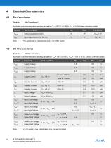
Electrical Characteristics Applicable over recommended operating range from TA = 25°C, f = 1.0MHz, VCC = +5.0V (unless otherwise noted). Symbol Test Conditions This parameter is characterized and is not 100% tested. Applicable over recommended operating range from: TAI = -40°C to +85°C, VCC = +1.8V to +5.5V, (unless otherwise noted). Symbol Supply Voltage Test Condition Supply Voltage Supply Voltage Supply Current Standby Current Standby Current Standby Current Input Leakage Output Leakage Input High Voltage Input High Voltage Output High Voltage Output High Voltage VIL min and VIH max are reference...
Open the catalog to page 4
Applicable over recommended operating range from TA = -40°C to + 85°C, Vcc = +2.7V to + 5.5V, CL = 1 TTL Gate and 100pF (unless otherwise noted). Note: 1. This parameter is ensured by characterization.
Open the catalog to page 5
Functional Description The AT93C46E is accessed via a simple and versatile three-wire serial communication interface. Device operation is controlled by seven instructions issued by the host processor. A valid instruction starts with a rising edge of CS and consists of a Start condition (Logic 1) followed by the appropriate opcode and the desired memory address location. Table 5-1. Reads data stored in memory, at specified address. Write enable must precede all programming modes. Erase memory location An A0. Writes memory location An A0. Erases all memory locations. Valid only at VCC = 4.5V to...
Open the catalog to page 6
WRITE ALL (WRAL): The Write All (WRAL) instruction programs all memory locations with the data patterns specified in the instruction. The DO pin outputs the Ready/Busy status of the part if CS is brought high after being kept low for a minimum of 250ns (tCS). The WRAL instruction is valid only at VCC = 5.0V 10%. Erase/Write Disable (EWDS): To protect against accidental data disturb, the Erase/Write Disable (EWDS) instruction disables all programming modes and should be executed after all programming operations. The operation of the Read instruction is independent of both the EWEN and EWDS instructions...
Open the catalog to page 7
Timing Diagrams Figure 6-1. Synchronous Data Timing Note: 1. This is the minimum SK period. Table 6-1. Organization Key for Timing Diagrams Figure 6-2. Read Timing
Open the catalog to page 8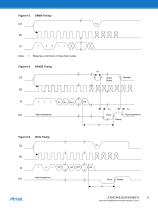
Note: 1. Requires a minimum of nine clock cycles. Figure 6-4. ERASE Timing Figure 6-5. Write Timing
Open the catalog to page 9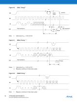
Note: 1. Valid only at Vcc = 4.5V to 5.5V. Notes: 1. Valid only at Vcc = 4.5V to 5.5V. 2. Requires a minimum of nine clock cycles. Note: 1. Requires a minimum of nine clock cycles.
Open the catalog to page 10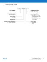
Ordering Code Detail AT 9 3 C 4 6 E N - S H - B Atmel Designator Shipping Carrier Option B or Blank = Bulk (Tubes) T = Tape and Reel Product Family 93C = Microwire-compatible 3-Wire Serial EEPROM Device Density 46 = 1 kilobit Device Revision Package Device Grade or Wafer/Die Thickness H = Green, NiPdAu Lead Finish Industrial Temperature Range (-40°C to +85°C) U = Green, Matte Sn Lead Finish Industrial Temperature Range (-40°C to +85°C) Package Variation (if applicable) Package Option N = 0.150” Wide JEDEC SOIC S = JEDEC SOIC T = TSSOP P = PDIP
Open the catalog to page 11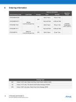
Ordering Information Delivery Information Atmel Ordering Code Lead Finish Bulk (Tubes) Bulk (Tubes) Bulk (Tubes) Operation Range NiPdAu (Lead-free/Halogen-free) 8-lead, 0.170” wide, Thin Shrink Small Outline Package (TSSOP) 8-lead, 0.150” wide, Plastic Gull Wing, Small Outline (JEDEC SOIC) 8-lead, 0.300” wide body, Plastic Dual In-line Package (PDIP)
Open the catalog to page 12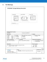
Part Markings AT93C46E: Package Marking Information ATMLHYWW ### % AAAAAAAA ATMLUYWW ### % AAAAAAAA HYWW ###% Note: Lot Number and location of assembly and on the bottom side of the package. Note 2: Package drawings are not to scale Catalog Number Truncation AT93C46E M = Month A: January B: February ... L: December WW = Work Week of Assembly 02: Week 2 04: Week 4 ... 52: Week 52 AAA...A = Atmel Wafer Lot Number Trace Code Grade/Lead Finish Material U: Industrial/Matte Tin/SnAgCu H: Industrial/NiPdAu Atmel Truncation AT: Atmel ATM: Atmel ATML: Atmel 3/13/14 93C46ESM, AT93C46E Package Marking Information...
Open the catalog to page 13All Atmel catalogs and technical brochures
 32-bit Microcontrollers
20 Pages
 MCUs Driving Displays
12 Pages
 Touch and 3D Gesture Control
12 Pages
 16-bit MCUs and DSCs
20 Pages
 XLP PIC® MCUs
8 Pages
 8-bit MCUs
16 Pages
 AT93C56B/66B Automotive
17 Pages
 Atmel AT86RF215 Device Family
235 Pages
 AT24C01C/02C
22 Pages
 maXTouch U Series - Flyer
2 Pages


Archived catalogs
 tinyAVR ATtiny24/44/84 Preliminary
240 Pages
 ATmega164P/324P/644P Preliminary
440 Pages
 ATmega48P/88P/168P/328P Preliminary
426 Pages
 ATmega1284P Preliminary
356 Pages
 AT90PWM216/316
359 Pages
 AT90PWM2, AT90PWM3, AT90PWM2B, AT90PWM3B
361 Pages
 ATmega329/3290/649/6490 Preliminary
392 Pages
 ATmega329P/3290P Preliminary
388 Pages
 AT90CAN32/64/128
428 Pages
 AT86RF230 Preliminary
98 Pages
 ATmega48/88/168 Automotive
335 Pages
 ATtiny25, ATtiny45, ATtiny85 Automotive
192 Pages
 ATtiny24/44/84 Automotive Preliminary
225 Pages
 AT86RF231 Preliminary
180 Pages
 Biometrics (Fingerprint Sensor)
20 Pages


- Transceiver module
- Potentiometer
- Industrial converter
- Ethernet transceiver
- Analog potentiometer
- Low-noise amplifier
- Microcontroller
- Analog amplifier
- Analog converter
- Circuit board
- Operational amplifier
- 32-bit microcontroller
- Low-power microcontroller
- Analog microcontroller
- High-speed converter
- General purpose microcontroller
- DAC converter
- Communication microcontroller
- High-speed amplifier
- ARM microcontroller