AT90PWM216/316

AT90PWM216/316
- 16K Bytes of In-System Programmable Flash with 10,000 write/erase cycles endurance.
- 512 Bytes of EEPROM with 100,000 write/erase cycles endurance.
- 1024 Bytes of internal SRAM.
- Operating voltage range: 2.7V - 5.5V.
- Operating temperature range: -40°C to +105°C.
- Advanced RISC architecture with 129 powerful instructions.
- 32 x 8 general-purpose working registers.
- On-chip 2-cycle multiplier.
- On-chip debug interface (debugWIRE).
- Two or three 12-bit high-speed Power Stage Controllers (PSC) with 4-bit resolution enhancement.
- One 8-bit and one 16-bit general-purpose Timer/Counter.
- Programmable Serial USART and Master/Slave SPI Serial Interface.
- 10-bit ADC with up to 11 single-ended channels and 2 differential channel pairs.
- 10-bit DAC and multiple analog comparators.
- Low power idle, noise reduction, and power-down modes.
- Power-on reset and programmable brown-out detection.
- Internal calibrated RC oscillator (8 MHz) and on-chip PLL for fast PWM and CPU operation.
Catalog excerpts
> High Performance, Low Power AVR ծ 8-bit Microcontroller > Advanced RISC ArchitectureՖ129 Powerful Instructions - Most Single Clock Cycle Execution32 x 8 General Purpose Working Registers֖Fully Static Operation Up to 1 MIPS throughput per MHz֖On-chip 2-cycle Multiplier > Data and Non-Volatile Program MemoryՖ16K Bytes Flash of In-System Programmable Program Memory Endurance: 10,000 Write/Erase CyclesՖOptional Boot Code Section with Independent Lock Bits > In-System Programming by On-chip Boot Program Օ > True Read-While-Write Operation512 Bytes of In-System Programmable EEPROM ֕ > Endurance: 100,000 Write/Erase Cycles1024 Bytes Internal SRAM ֖Programming Lock for Flash Program and EEPROM Data Security > On Chip Debug Interface (debugWIRE) Օ > Peripheral FeaturesTwo or three 12-bit High Speed PSC (Power Stage Controllers) with 4-bit Resolution Enhancement֕Non Overlapping Inverted PWM Output Pins With Flexible Dead-Time Variable PWM duty Cycle and Frequency ՕSynchronous Update of all PWM RegistersAuto Stop Function for Event Driven PFC ImplementationՕLess than 25 Hz Step Width at 150 kHz Output Frequency PSC2 with four Output Pins and Output MatrixՖOne 8-bit General purpose Timer/Counter with Separate Prescaler and Capture ModeOne 16-bit General purpose Timer/Counter with Separate Prescaler, Compare Mode and Capture Mode֖Programmable Serial USARTStandard UART mode Օ16/17 bit Biphase Mode for DALI CommunicationsMaster/Slave SPI Serial Interface ֖10-bit ADCUp To 11 Single Ended Channels and 2 Fully Differential ADC Channel PairsՕProgrammable Gain (5x, 10x, 20x, 40x on Differential Channels) Internal Reference VoltageՖ10-bit DACTwo or three Analog Comparator with Resistor-Array to Adjust Comparison Voltage֖4 External Interrupts Programmable Watchdog Timer with Separate On-Chip Oscillator ֕ > Special Microcontroller FeaturesLow Power Idle, Noise Reduction, and Power Down Modes֖Power On Reset and Programmable Brown Out Detection Flag Array in Bit-programmable I/O Space (4 bytes) 7710C֖AVR01/08 size="-2">
Open the catalog to page 1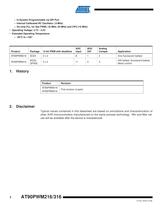
In-System Programmable via SPI Port֖Internal Calibrated RC Oscillator ( 8 MHz)On-chip PLL for fast PWM ( 32 MHz, 64 MHz) and CPU (16 MHz) > Extended Operating Temperature: Ֆ-40C to +105а ProductPackage12 bit PWM with deadtimeADC InputADC DiffAnalog ComparApplication AT90PWM216SO242 x 2812One fluorescent ballastAT90PWM316SO32, QFN32 3 x 21123HID ballast, fluorescent ballast, Motor control > ProductRevision AT90PWM216AT90PWM316First revision of parts >
Open the catalog to page 2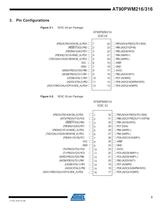
Figure 3-1. SOIC 24-pin Package Figure 3-2. SOIC 32-pin Package 3 > 7710CAVR֖01/08 size="-1">
Open the catalog to page 3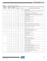
S024 Pin NumberSO32 Pin NumberQFN32 Pin NumberMnemonicTypeName, Function & Alternate Function 684VCCpower Power Supply: 172319AVCCPower Analog Power Supply: This is the power supply voltage for analog partFor a normal use this pin must be connected.192521AREFPower Analog Reference : reference for analog converter . This is the reference voltage of the A/D converter. As output, can be used by external analog8128PBOI/OMISO (SPI Master In Slave Out)PSCOUT20 output9139PB1I/OMOSI (SPI Master Out Slave In)PSCOUT21 output162016PB2I/OADC5 (Analog Input Channel5 )INT1202723PB3I/OAMP0- (Analog Differential...
Open the catalog to page 5
Table 3-1. Pin out description (Continued) > S024 Pin NumberSO32 Pin NumberQFN32 Pin NumberMnemonicTypeName, Function & Alternate Function 1129PD0I/OPSCOUT00 outputXCK (UART Transfer Clock) SS_A (Alternate SPI Slave Select)3432PD1I/OPSCIN0 (PSC 0 Digital Input )CLKO (System Clock Output)451PD2I/OPSCIN2 (PSC 2 Digital Input) OC1A (Timer 1 Output Compare A) MISO_A (Programming & alternate SPI Master In Slave Out)562PD3I/OTXD (Dali/UART Tx data)OC0A (Timer 0 Output Compare A) SS (SPI Slave Select) MOSI_A (Programming & alternate Master Out SPI Slave In)121612PD4I/OADC1 (Analog Input Channel 1)RXD...
Open the catalog to page 6
The Idle mode stops the CPU while allowing the SRAM, Timer/Counters, SPI ports and interruptsystem to continue functioning. The Power-down mode saves the register contents but freezesthe Oscillator, disabling all other chip functions until the next interrupt or Hardware Reset. TheADC Noise Reduction mode stops the CPU and all I/O modules except ADC, to minimize switch-ing noise during ADC conversions. In Standby mode, the Crystal/Resonator Oscillator is runningwhile the rest of the device is sleeping. This allows very fast start-up combined with low power consumption. The device is manufactured...
Open the catalog to page 8
4.2.5Port D (PD7..PD0) Port D is an 8-bit bi-directional I/O port with internal pull-up resistors (selected for each bit). ThePort D output buffers have symmetrical drive characteristics with both high sink and sourcecapability. As inputs, Port D pins that are externally pulled low will source current if the pull-upresistors are activated. The Port D pins are tri-stated when a reset condition becomes active, even if the clock is not running.Port D also serves the functions of various special features of the AT90PWM216/316 as listedon page 73. 4.2.6Port E (PE2..0) RESET/ XTAL1/XTAL2 Port E is...
Open the catalog to page 9
The fast-access Register File contains 32 x 8-bit general purpose working registers with a singleclock cycle access time. This allows single-cycle Arithmetic Logic Unit (ALU) operation. In a typ-ical ALU operation, two operands are output from the Register File, the operation is executed,and the result is stored back in the Register File in one clock cycle.Six of the 32 registers can be used as three 16-bit indirect address register pointers for DataSpace addressing ֖ enabling efficient address calculations. One of the these address pointers can also be used as an address pointer for look up...
Open the catalog to page 11
Figure 5-4. The Parallel Instruction Fetches and Instruction Executions Figure 5-5 shows the internal timing concept for the Register File. In a single clock cycle an ALUoperation using two register operands is executed, and the result is stored back to the destina- tion register. > T1T2T3T4 clk1st Instruction Fetch1st Instruction Execute2nd Instruction Fetch2nd Instruction Execute3rd Instruction Fetch3rd Instruction Execute4th Instruction Fetch CPU Figure 5-5. Single Cycle ALU Operation > T1T2T3T4 clk CPU Total Execution TimeRegister Operands FetchALU Operation ExecuteResult Write Back The AVR...
Open the catalog to page 15All Atmel catalogs and technical brochures
 32-bit Microcontrollers
20 Pages
 MCUs Driving Displays
12 Pages
 Touch and 3D Gesture Control
12 Pages
 16-bit MCUs and DSCs
20 Pages
 XLP PIC® MCUs
8 Pages
 8-bit MCUs
16 Pages
 AT93C56B/66B Automotive
17 Pages
 Atmel AT86RF215 Device Family
235 Pages
 AT24C01C/02C
22 Pages
 maXTouch U Series - Flyer
2 Pages


Archived catalogs
 tinyAVR ATtiny24/44/84 Preliminary
240 Pages
 ATmega164P/324P/644P Preliminary
440 Pages
 ATmega48P/88P/168P/328P Preliminary
426 Pages
 ATmega1284P Preliminary
356 Pages
 AT90PWM2, AT90PWM3, AT90PWM2B, AT90PWM3B
361 Pages
 ATmega329/3290/649/6490 Preliminary
392 Pages
 ATmega329P/3290P Preliminary
388 Pages
 AT90CAN32/64/128
428 Pages
 AT86RF230 Preliminary
98 Pages
 ATmega48/88/168 Automotive
335 Pages
 ATtiny25, ATtiny45, ATtiny85 Automotive
192 Pages
 ATtiny24/44/84 Automotive Preliminary
225 Pages
 AT86RF231 Preliminary
180 Pages
 Biometrics (Fingerprint Sensor)
20 Pages


- Transceiver module
- Potentiometer
- Industrial converter
- Ethernet transceiver
- Analog potentiometer
- Low-noise amplifier
- Analog amplifier
- Circuit board
- Operational amplifier
- 32-bit microcontroller
- Low-power microcontroller
- Analog microcontroller
- High-speed converter
- General purpose microcontroller
- DAC converter
- Communication microcontroller
- High-speed amplifier
- ARM microcontroller