AT86RF231 Preliminary
1 /180Pages

AT86RF231 Preliminary
1 /180Pages
Catalog excerpts

> High Performance RF-CMOS 2.4 GHz Radio Transceiver Targeted for IEEE 802.15.4 ՙ , ZigBee and ISM Applications ٕ > Industry Leading Link Budget (104 dB)Receiver Sensitivity -101 dBm ֖Programmable Output Power from -17 dBm up to +3 dBm > Ultra-Low Current Consumption: Ֆ SLEEP = 0.02 A Ֆ TRX_OFF = 0.4 mA RX_ON = 13.2 mA ֖ BUSY_TX = 14.3 mA (at max. Transmit Power of +3 dBm) > Ultra-Low Supply Voltage (1.8V to 3.6V) with Internal Regulator Օ > Optimized for Low BoM Cost and Ease of Production:Few External Components Necessary (Crystal, Capacitors and Antenna)֖Excellent ESD Robustness > Easy to Use Interface:ՖRegisters, Frame Buffer and AES Accessible through Fast SPIOnly Two Microcontroller GPIO Lines Necessary֖One Interrupt Pin from Radio TransceiverClock Output with Prescaler from Radio Transceiver ֕ > Radio Transceiver Features:128-byte FIFO (SRAM) for Data Buffering֖Programmable Clock Output, to Clock the Host Microcontroller or as Timer ReferenceIntegrated RX/TX Switch֖Fully Integrated, Fast Settling PLL to support Frequency HoppingBattery Monitor֖Fast Wake-Up Time < 0.25 msec > Special IEEE 802.15.4-2006 Hardware Support:ՖFCS Computation and Clear Channel AssessmentRSSI Measurement, Energy Detection and Link Quality Indication ֕ > MAC Hardware Accelerator:Automated Acknowledgement, CSMA-CA and Retransmission֖Automatic Address FilteringAutomated FCS Check ֕ > Extended Feature Set Hardware Support:AES 128bit Hardware Accelerator֖RX/TX Indication (external RF Front-End Control)RX Antenna Diversity ֖Supported PSDU data rates: 250 kb/s, 500 kb/s, 1 Mb/s and 2 Mb/sTrue Random Number Generation for Security Application ֕ > Industrial Temperature Range:-40ְ C to +85 C Е > I/O and Packages:32-pin Low-Profile QFN Package 5 x 5 x 0.9 mmֳRoHS/Fully Green ֕ > Compliant to IEEE 802.15.4-2006 and IEEE 802.15.4-2003 > Compliant to EN 300 328/440, FCC-CFR-47 Part 15, ARIB STD-66, RSS-210 8111AՖAVR05/08 size="-4">
Open the catalog to page 1
Figure 1-1. AT86RF231 Pin-out Diagram XTAL2XTAL1 AVSSEVDDAVDDAVSSAVSSAVSS 322423222120191817 12345678 31302928272625 910111213141516 exposed paddle AVSS AT 86 RF 231 > SCLKMISODVSSMOSI/SELIRQ CLKMDVSSDIG3DIG4AVSSAVSSRFPRFNDVSS/RST DIG1DIG2SLP_TRDVSSDVDDDVDDDEVDDDVSS Note:The exposed paddle is electrically connected to the die inside the package. It shall be soldered to the board to ensure electrical and thermal contact and good mechanical stability. 2
Open the catalog to page 2
Table 1-1. Pin Description AT86RF231 > PinsNameTypeDescription 1DIG3Digital output (Ground)1. RX/TX Indicator, see Section 11.52. If disabled, pull-down enabled (AVSS) > 2DIG4Digital output (Ground)1. RX/TX indicator (DIG3 inverted), see Section 11.52. If disabled, pull-down enabled (AVSS)3AVSSGroundGround for RF signals4RFPRF I/ODifferential RF signal 5RFNRF I/ODifferential RF signal6AVSSGroundGround for RF signals7DVSSGroundDigital ground 8/RSTDigital inputChip reset; active low9DIG1Digital output (Ground)1. Antenna Diversity RF switch control, see Section 11.42. If disabled, pull-down enabled...
Open the catalog to page 3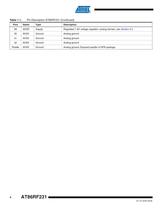
Table 1-1. Pin Description AT86RF231 (Continued) > PinsNameTypeDescription 29AVDDSupplyRegulated 1.8V voltage regulator; analog domain, see Section 9.430AVSSGroundAnalog ground31AVSSGroundAnalog ground32AVSSGroundAnalog groundPaddleAVSSGroundAnalog ground; Exposed paddle of QFN package 4 >
Open the catalog to page 4
PinValues and ConditionsComments > DC = 0.9V (BUSY_TX)V RFP/RFNV > DC = 20 mV (receive states)V > DC = 0 mV (otherwise)DC level at pins RFP/RFN for various transceiver statesAC coupling is required if an antenna with a DC path to ground is used. Serial capacitance and capacitance of each pin to ground must be < 30pF.XTAL1/ XTAL2V > DC = 0.9V at both pinsC ) of the pins must be considered as additional load capacitance to the crystal.DVDDV > PAR = 3 pFDC level at pins XTAL1/XTAL2 for various transceiver statesParasitic capacitance (C > PAR DC = 1.8V (all states, except SLEEP)V > DC = 0 mV (otherwise)DC...
Open the catalog to page 6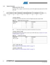
1.3.3Register DescriptionRegister 0x03 (TRX_CTRL_0): The TRX_CTRL_0 register controls the drive current of the digital output pads and the CLKMclock rate. > Bit76543210 PAD_IOPAD_IO_CLKMCLKM_SHA_SELCLKM_CTRLTRX_CTRL_0 Read/WriteR/WR/WR/WR/WR/WR/WR/WR/W Initial Value00011001 Bit [7:6] - PAD_IO The register bits set the output driver current of all digital output pads, except CLKM. Table 1-5. Digital Output Driver Strength > Register BitValueDescription PAD_IO0 (1) 2 mA14 mA26 mA38 mA Note:1.Reset values of register bits are underlined characterized in the document. ՕBit [5:6] - PAD_IO_CLKM The...
Open the catalog to page 8
Typical values contained in this datasheet are based on simulations and testing. Min and Maxvalues are available when the radio transceiver has been fully characterized. > The AT86RF231 is a feature rich, low-power 2.4 GHz radio transceiver designed for industrialand consumer ZigBee/IEEE 802.15.4 and high data rate 2.4 GHz ISM band applications. Theradio transceiver is a true SPI-to-antenna solution. All RF-critical components except theantenna, crystal and de-coupling capacitors are integrated on-chip. Therefore, the AT86RF231 is particularly suitable for applications like:2.4 GHz IEEE 802.15.4...
Open the catalog to page 9
An internal 128-byte RAM for RX and TX (Frame Buffer) buffers the data to be transmitted or thereceived data.The configuration of the AT86RF231, reading and writing of Frame Buffer is controlled by theSPI interface and additional control lines.The AT86RF231 further contains comprehensive hardware-MAC support (Extended OperatingMode) and a security engine (AES) to improve the overall system power efficiency and timing.The stand-alone 128-bit AES engine can be accessed in parallel to all PHY operational transac-tions and states using the SPI interface, except during SLEEP state.For applications...
Open the catalog to page 11
control pins DIG1/DIG2, the RF signal is amplified by an optional low-noise amplifier (N2) andfed to the radio transceiver using the second RX/TX switch (SW1).During transmit the AT86RF231 TX signal is amplified using an external PA (N1) and fed to theantennas via an RF switch (SW2). In this example RF switch SW2 further supports AntennaDiversity controlled by the differential pin pair DIG1/DIG2.The security engine (AES) and High Data Rate Modes do not require specific circuitry to oper-ate. The security engine (AES) has to be configured in advance, for details refer to Section 11.1Security Module...
Open the catalog to page 15All Atmel catalogs and technical brochures
 32-bit Microcontrollers
20 Pages
 MCUs Driving Displays
12 Pages
 Touch and 3D Gesture Control
12 Pages
 16-bit MCUs and DSCs
20 Pages
 XLP PIC® MCUs
8 Pages
 8-bit MCUs
16 Pages
 AT93C56B/66B Automotive
17 Pages
 Atmel AT86RF215 Device Family
235 Pages
 AT24C01C/02C
22 Pages
 maXTouch U Series - Flyer
2 Pages


Archived catalogs
 tinyAVR ATtiny24/44/84 Preliminary
240 Pages
 ATmega164P/324P/644P Preliminary
440 Pages
 ATmega48P/88P/168P/328P Preliminary
426 Pages
 ATmega1284P Preliminary
356 Pages
 AT90PWM216/316
359 Pages
 AT90PWM2, AT90PWM3, AT90PWM2B, AT90PWM3B
361 Pages
 ATmega329/3290/649/6490 Preliminary
392 Pages
 ATmega329P/3290P Preliminary
388 Pages
 AT90CAN32/64/128
428 Pages
 AT86RF230 Preliminary
98 Pages
 ATmega48/88/168 Automotive
335 Pages
 ATtiny25, ATtiny45, ATtiny85 Automotive
192 Pages
 ATtiny24/44/84 Automotive Preliminary
225 Pages
 Biometrics (Fingerprint Sensor)
20 Pages


- Potentiometer
- Industrial converter
- Ethernet transceiver
- Analog potentiometer
- Analog amplifier
- Analog converter
- Circuit board
- Operational amplifier
- 32-bit microcontroller
- Low-power microcontroller
- Analog microcontroller
- High-speed converter
- General purpose microcontroller
- DAC converter
- Communication microcontroller
- High-speed amplifier
- ARM microcontroller