Overview: The AT86RF230 is a low-power 2.4 GHz radio
transceiver designed for ZigBee and IEEE 802.15.4 applications. It integrates most RF-critical components on-chip, requiring minimal external components such as an antenna, crystal, and capacitors. This makes it suitable for wireless sensor networks, industrial control, home automation, and more.
Features: The transceiver offers a high link budget of 104 dB, programmable output power from -17 dBm to 3 dBm, and receiver sensitivity of -101 dBm. It operates on ultra-low power with a sleep mode consumption of 20 nA and supports a supply voltage range of 1.8V to 3.6V. The device is compliant with various standards including IEEE 802.15.4-2003 and FCC regulations.
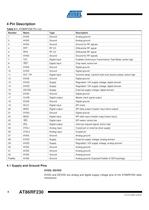
Pin Description: The AT86RF230 features a 32-pin QFN package with various pins for analog and digital ground, RF I/O, SPI interface, and control signals. Key pins include RFP/RFN for differential RF signals, XTAL1/XTAL2 for crystal connections, and digital interface pins for SPI communication.
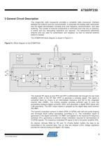
General Circuit Description: The transceiver includes an analog radio transceiver and digital demodulation components. It supports offset-QPSK modulation and features an internal 128-byte RAM for data buffering. The device also includes integrated voltage regulators and a PLL for frequency synthesis.
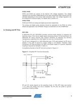
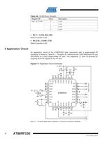
Application Circuit: An example application circuit includes a balun for RF port transformation, decoupling capacitors for power supply stability, and a crystal oscillator setup for frequency accuracy. The design emphasizes minimizing parasitic capacitance and separating ground planes for optimal performance.
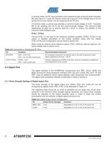
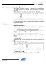
Driver and Configuration: The digital output driver strength is configurable, with options ranging from 2 mA to 8 mA. Pull-up and pull-down configurations are available for digital input pins, and the device includes registers for controlling various operational parameters.
Recommendations: For best performance, ensure low-resistance and low-inductance connections for capacitors, avoid crosstalk by careful routing of crystal and RF lines, and separate power domains on the PCB.
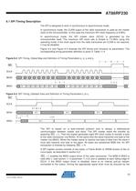
Microcontroller Interface Overview: The document describes the interface between the AT86RF230 radio transceiver and a microcontroller, focusing on the SPI (Serial Peripheral Interface) and additional control signals. The interface includes signals such as MOSI, MISO, SCLK, CLKM, IRQ, and SLP_TR, which are crucial for communication and control.
SPI Timing and Protocol: The SPI can operate in synchronous or asynchronous modes. In synchronous mode, the CLKM output is used as the master clock, with a maximum frequency of 8 MHz. In asynchronous mode, the microcontroller generates the clock, limited to 7.5 MHz. The SPI protocol is byte-oriented, with transactions initiated by asserting the SEL signal low.
SPI Protocol Details: The SPI protocol includes various access modes: Register Access, Frame Buffer Access, and SRAM Access. Each mode has specific command byte structures and data transfer sequences. Register Access involves two-byte read/write operations, while Frame Buffer Access is used for uploading or downloading frames. SRAM Access allows access to specific bytes within the Frame Buffer, reducing SPI traffic.
Radio Transceiver Identification: The AT86RF230 can be identified using four registers containing the part number, version number, and JEDEC manufacturer ID. These registers provide essential identification information for the transceiver.
SLP_TR Signal Functionality: The SLP_TR signal is multifunctional, with its role depending on the transceiver's state. It is used for sleep/wake-up transitions and initiating transmissions. The document outlines the state transitions and the impact of the SLP_TR signal on the transceiver's operation.
Conclusion: This technical document provides a comprehensive overview of the AT86RF230's interface with a microcontroller, detailing the SPI protocol, signal descriptions, and transceiver identification. It also explains the functionality of the SLP_TR signal in managing power states and initiating transmissions.
Specifications and Procedures: The document outlines the operation of the AT86RF230 radio transceiver, focusing on its power-down modes, interrupt logic, and operating modes. The transceiver supports a power-down mode for receive states RX_ON and RX_AACK_ON, allowing the microcontroller to power down without missing incoming frames. This is achieved by manipulating the SLP_TR pin, which affects the CLKM output and transceiver states.
Interrupt Logic: The AT86RF230 differentiates between six interrupt events, managed via the IRQ_MASK register. Interrupts are combined into one external line (IRQ), and the status is read from the IRQ_STATUS register. Key interrupts include BAT_LOW, TRX_UR, TRX_END, RX_START, PLL_UNLOCK, and PLL_LOCK, each indicating specific operational states or errors.
Operating Modes: The document details the Basic Operating Mode, designed for IEEE 802.15.4 applications, which includes states like P_ON, SLEEP, TRX_OFF, PLL_ON, RX_ON, RX_ON_NOCLK, and BUSY_TX. Each state has specific functions and transitions, controlled by signal pins and register commands. The SLEEP state minimizes power consumption, while RX_ON_NOCLK allows the microcontroller to power down during frame listening.
State Control and Timing: State transitions are controlled by the SLP_TR and RST pins, and the TRX_STATE register. The document emphasizes the importance of confirming state changes by reading the TRX_STATUS register. Timing details for state transitions, power-on, and wake-up procedures are provided, ensuring precise control over the transceiver's operation.
Interrupt Handling: In Basic Operating Mode, interrupts like RX_START and TRX_END support RX and TX operations, indicating the start and completion of frame reception or transmission. The document includes timing diagrams to illustrate these processes.
Conclusion: The AT86RF230 offers flexible power management and precise control over radio transceiver states, supported by a robust interrupt system. Understanding these specifications and procedures is crucial for optimizing performance in IEEE 802.15.4 applications.
Specifications and Procedures: The document outlines the operational procedures and specifications for the AT86RF230 radio transceiver. Key states include P_ON, TRX_OFF, PLL_ON, and RX_ON, each with specific transition timings and conditions. The transition from P_ON to TRX_OFF takes 880 µs, influenced by external capacitors and oscillator setup. The reset procedure involves setting RST to low, initializing calibration cycles, and entering TRX_OFF state.
State Transition Timing: State transitions are detailed with typical and worst-case timings. For example, TRX_OFF to PLL_ON takes 180 µs, while PLL_ON to RX_ON is 1 µs. These timings are crucial for ensuring proper operation under varying conditions.
Register Descriptions: Registers like TRX_STATUS and TRX_STATE control and signal the transceiver's state. TRX_STATUS indicates the current state and transition progress, while TRX_CMD in TRX_STATE initiates state transitions.
Extended Operating Mode: This mode supports IEEE 802.15.4-2003 standards, offering features like automatic acknowledgment (RX_AACK) and frame retransmission (TX_ARET). It enhances efficiency by reducing code size and simplifying time-critical tasks.
RX_AACK and TX_ARET Transactions: RX_AACK involves frame reception, address filtering, and automatic ACK transmission. TX_ARET includes CSMA-CA, frame transmission, and automatic retries. These processes ensure reliable communication by handling acknowledgments and retransmissions automatically.
Configuration Requirements: For RX_AACK and TX_ARET modes, specific registers must be configured, including PAN-ID, IEEE addresses, and CSMA-CA parameters. Proper configuration ensures compliance with IEEE standards and optimal transceiver performance.
Specifications and Procedures: The document details the operation of the AT86RF230 radio transceiver, focusing on its RX_AACK and TX_ARET functionalities. RX_AACK is used for automatic acknowledgment reception, while TX_ARET involves transmitting with automatic CSMA-CA retry. The TX_ARET process begins with a command or pin signal, executing the CSMA-CA algorithm to ensure a clear channel before transmission. If an acknowledgment (ACK) is expected and not received, the process retries until successful or the maximum retries are reached.
Interrupt Handling: In Extended Operating Mode, interrupt handling is minimized to reduce power consumption. Key interrupts include TRX_END for transaction completion and RX_START for frame reception. Some interrupts like PLL_UNLOCK and PLL_LOCK are disabled for regular operation.
Register Summary: The document provides a comprehensive summary of control and address registers. Key registers include TRX_STATUS for transceiver status, TRX_STATE for state control, and XAH_CTRL for retry value control. The CSMA_SEED registers are used for the CSMA-CA algorithm, while address registers (SHORT_ADDR, PAN_ID, IEEE_ADDR) are used for address filtering.
Recommendations and Best Practices: It is recommended to download transmit data before starting a TX_ARET transaction. The document also advises on setting specific register bits for optimal operation, such as MIN_BE for back-off exponent and I_AM_COORD for PAN coordinator identification.
Key Parameters and Limitations: Parameters like MAX_FRAME_RETRIES and MAX_CSMA_RETRIES control the number of retries for frame transmission and channel access. The document specifies timing constraints and processing delays for various operations, ensuring precise synchronization and efficient power management.
IEEE Address Registers: Registers 0x27 to 0x2B are used for storing the 64-bit IEEE address for address filtering. Each register holds 8 bits of the address, with all bits being read/write capable and having a reset value of 0.
Frame Format and Protocol Layers: The document describes the frame structure as per the IEEE 802.15.4-2003 standard, detailing both the PHY and MAC layer structures. The PHY Protocol Layer Data Unit (PPDU) includes a Synchronization Header (SHR), a PHY Header (PHR), and a PHY Payload (PSDU). The MAC Protocol Layer Data Unit (MPDU) consists of a MAC Header (MHR), a MAC Service Data Unit (MSDU), and a MAC Footer (MFR).
Frame Check Sequence (FCS): The FCS is a 16-bit cyclic redundancy check used to detect errors in frames. It is automatically evaluated during reception and can be generated during transmission. The FCS is calculated using a specific polynomial and is appended to the frame.
Automatic FCS Generation and Checking: The AT86RF230 can automatically generate and check the FCS. The TX_AUTO_CRC_ON bit in the PHY_TX_PWR register enables automatic FCS generation. The RX_CRC_VALID bit in the PHY_RSSI register indicates the validity of the FCS for received frames.
Energy Detection (ED): The Energy Detection module measures the received signal power, with 85 unique energy levels and 1 dB resolution. ED measurements can be initiated manually or automatically and are stored in the PHY_ED_LEVEL register.
Register Descriptions: Several registers are described, including PHY_TX_PWR for setting transmit power and controlling FCS, PHY_RSSI for indicating received signal strength and FCS validity, and PHY_ED_LEVEL for storing ED measurement results.
Specifications: The document outlines the specifications of the AT86RF230 transceiver, focusing on its Received Signal Strength Indicator (RSSI), Link Quality Indication (LQI), and Clear Channel Assessment (CCA) features. The RSSI has a sensitivity of -91 dBm and a dynamic range of 81 dB, with values ranging from 0 to 28. The LQI measures the quality of received packets, ranging from 0 to 255, and is used to assess packet error rates. The CCA module supports three modes for detecting clear channels, with adjustable energy detection thresholds.
Procedures: Manual Energy Detection (ED) measurements can be initiated via register access. RSSI values are updated every 2 µs and stored in the PHY_RSSI register. LQI values are appended to received frames and can be read from the Frame Buffer. CCA requests are initiated by setting specific register bits, with results available after 140 µs.
Data Interpretation: RSSI values indicate received signal strength, with calculations provided for converting RSSI values to RF input power. LQI values correlate with packet error rates, with higher values indicating better signal quality. CCA results indicate channel status, with specific register bits signaling completion and channel activity.
Register Descriptions: The document details various registers, such as PHY_RSSI, TRX_STATUS, PHY_CC_CCA, and CCA_THRES, explaining their roles in signal strength measurement, channel assessment, and configuration settings.
Recommendations: For optimal performance, it is recommended to use automatically generated ED values in Extended Operating Mode and to avoid manual CCA measurements in this mode. High LQI values should guide routing decisions in ZigBee networks, while RSSI/ED values help differentiate links with similar LQI values.
Output Power Settings: The document provides a table listing register bits and corresponding output power levels in dBm for the AT86RF230 transceiver. The values range from -5.2 dBm to -17.2 dBm.
Frame Buffer: The AT86RF230 features a 128-byte dual-port SRAM frame buffer, accessible via SPI and TX/RX BBP ports. It supports IEEE 802.15.4-2003 frames and requires the digital voltage regulator to be active, except in SLEEP and P_ON states. Data management involves ensuring no new frames overwrite existing data unless intended. The buffer's content is preserved across state changes except when entering SLEEP mode.
Voltage Regulators: The AT86RF230 includes internal voltage regulators for analog and digital domains, providing a 1.8V supply. These can be configured via the VREG_CTRL register to use either internal or external regulators. The status of these regulators is indicated by AVDD_OK and DVDD_OK bits.
Battery Monitor: The battery monitor detects low supply voltage by comparing it to a programmable threshold. It issues a BAT_LOW interrupt if the voltage drops below this threshold. The BATMON register configures the monitor, and the BATMON_OK bit indicates the voltage status.
Crystal Oscillator: The AT86RF230 uses a 16 MHz crystal oscillator as a reference frequency source. The oscillator's performance is crucial for system accuracy, and it can be configured using the XOSC_CTRL register. The setup includes internal trimming capacitors to adjust frequency deviations.
Overview: The document provides technical specifications and operational guidelines for the AT86RF230 radio transceiver, focusing on its crystal oscillator, frequency synthesizer, and operational procedures.
Crystal Oscillator: The AT86RF230 includes a magnitude control circuit to ensure stable operation across different conditions and crystal types. Crystals with higher load capacitance are less sensitive to parasitic effects but result in longer start-up times and higher steady-state current consumption. The document provides a schematic for external component connections and instructions for setting up an external reference frequency.
Master Clock Signal Output (CLKM): The CLKM can output various frequencies (16 MHz, 8 MHz, 4 MHz, 2 MHz, or 1 MHz) and is configurable via register 0x03 (TRX_CTRL_0). Recommendations include turning off the CLKM when not in use to reduce power consumption.
Frequency Synthesizer (PLL): The PLL supports 16 channels in the IEEE 802.15.4 - 2.4 GHz band, with a channel spacing of 5 MHz. It features autonomous calibration loops for stable operation and includes interrupts for status indication. Manual calibration is recommended every 5 minutes or when significant temperature changes occur.
Automatic Filter Tuning (FTN): The filter-tuning unit ensures correct SSBF transfer function and PLL loop-filter time constant, independent of temperature and part variations.
Radio Transceiver Usage: Procedures for receiving and transmitting frames are detailed, including timing considerations and interrupt handling. The document emphasizes the importance of protocol timing and provides diagrams for frame receive and transmit procedures.
Technical Parameters: The document lists absolute maximum ratings and recommended operating ranges, highlighting the importance of adhering to these specifications to avoid device damage.
Digital Pin Specifications: The document outlines the digital pin specifications for the AT86RF230, including high and low-level input and output voltages. The high-level input voltage is specified as VDD - 0.4V, and the low-level input voltage is 0.4V. Similarly, the high-level output voltage is VDD - 0.4V, and the low-level output voltage is 0.4V.
Digital Interface Timing Specifications: The timing parameters for the digital interface are detailed, with a synchronous SCLK frequency of 8 MHz and an asynchronous frequency of 7.5 MHz. Various setup and hold times for signals like MOSI and MISO are specified, along with idle times and pulse widths.
General RF Specifications: The RF parameters include a frequency range of 2405 to 2480 MHz and a bit rate of 250 kbit/s. The reference oscillator frequency is 16 MHz, with a settling time of 0.5 to 1 ms. The document specifies a TX signal bandwidth of 2.8 MHz.
Transmitter Specifications: The transmitter section specifies an output power range of 0 to 6 dBm, with a power tolerance of ±3 dB. Harmonics and spurious emissions are detailed, complying with various standards like EN 300 328/440 and FCC-CFR-47 part 15.
Receiver Specifications: Receiver sensitivity is noted at -101 dBm, with various rejection parameters for adjacent channels. The document also specifies spurious emissions and carrier frequency offset tolerances.
Current Consumption Specifications: Current consumption is detailed for various states like transmit, receive, TRX_OFF, and SLEEP, with values ranging from 0.02 µA in SLEEP state to 16.5 mA in transmit state at 3 dBm output power.
Crystal Parameter Requirements: The crystal frequency is set at 16 MHz, with load capacitance between 8 to 14 pF and series resistance up to 100 Ω.
Register Reference: The AT86RF230 features 64 8-bit registers for configuration and control. A summary of non-reserved registers is provided, along with their functions and reset values.
Ordering Information: The document provides ordering codes and package details, specifying a voltage range of 1.8V to 3.6V and an industrial temperature range of -40°C to +85°C.
Soldering and Thermal Properties: Recommended soldering profiles and thermal resistance values are provided, with specific guidelines for package handling.
Appendix A - Continuous Transmission Test Mode: This section describes the continuous transmission test mode for application and certification tests, detailing configuration steps and programming sequences for both PRBS and CW modes.
Overview: The document provides technical details and operational procedures for the AT86RF230 transceiver. It includes specifications, procedures for setting registers, and handling various operational modes.
Specifications and Procedures: The document outlines specific register settings and pin configurations necessary for different operations, such as signal measurement and continuous transmission test mode. Key procedures include writing specific values to registers, setting pin states, and configuring transmission modes.
Errata and Workarounds: The document lists known issues with the AT86RF230 and provides workarounds. Notable issues include incorrect acknowledgment of broadcast frames, frame upload problems, and sensitivity to continuous wave interferers. Workarounds involve software modifications and specific register settings.
Continuous Transmission Test Mode: This mode is not characterized by Atmel and is not guaranteed. Normal operation is only assured when the TST pin is set to logic low.
Data Sheet Revision History: The document includes a history of revisions, highlighting changes such as updates to the SPI interface and operating mode diagrams.
References: The document references IEEE and ESD standards relevant to the AT86RF230's operation and testing.
Overview: The document is a technical datasheet for the AT86RF230, a radio transceiver. It provides detailed specifications, configurations, and operational procedures for the device.
Transmitter (TX): This section includes an overview, configuration details, and register descriptions necessary for setting up and operating the transmitter component of the AT86RF230.
Frame Buffer: Discusses data management, user-accessible content, and interrupt handling related to the frame buffer, which is crucial for managing data frames in the transceiver.
Voltage Regulators (AVREG, DVREG): Provides an overview and configuration instructions for the voltage regulators, along with data interpretation and register descriptions.
Battery Monitor (BATMON): Covers the overview, data interpretation, interrupt handling, and register descriptions for monitoring battery status.
Crystal Oscillator (XOSC): Details the setup of integrated and external reference frequency oscillators, master clock signal output, and associated register descriptions.
Frequency Synthesizer (PLL): Includes an overview, RF channel selection, calibration loops, interrupt handling, and register descriptions for the frequency synthesizer.
Automatic Filter Tuning (FTN): Briefly mentioned, indicating its role in the transceiver's operation.
Radio Transceiver Usage: Describes procedures for receiving and transmitting frames, essential for the device's communication functions.
Technical Parameters: Lists absolute maximum ratings, recommended operating ranges, digital pin specifications, interface timing, RF specifications, and current consumption details.
Register Reference: Provides a comprehensive reference for all registers used in the AT86RF230.
Appendices: Includes continuous transmission test mode and errata for different revisions of the AT86RF230.
Additional Information: Contains ordering information, soldering guidelines, package thermal properties, and a package drawing.
Disclaimer: Legal disclaimers regarding the use of the document and Atmel's liability.

 32-bit Microcontrollers
 MCUs Driving Displays
 Touch and 3D Gesture Control
 16-bit MCUs and DSCs
 XLP PIC® MCUs
 8-bit MCUs
 AT93C56B/66B Automotive
 Atmel AT86RF215 Device Family
 AT24C01C/02C
 maXTouch U Series - Flyer


 tinyAVR ATtiny24/44/84 Preliminary
 ATmega164P/324P/644P Preliminary
 ATmega48P/88P/168P/328P Preliminary
 ATmega1284P Preliminary
 AT90PWM216/316
 AT90PWM2, AT90PWM3, AT90PWM2B, AT90PWM3B
 ATmega329/3290/649/6490 Preliminary
 ATmega329P/3290P Preliminary
 AT90CAN32/64/128
 ATmega48/88/168 Automotive
 ATtiny25, ATtiny45, ATtiny85 Automotive
 ATtiny24/44/84 Automotive Preliminary
 AT86RF231 Preliminary
 Biometrics (Fingerprint Sensor)


