AT42QT1040 4-channel QTouch® Sensor IC
1 /22Pages

AT42QT1040 4-channel QTouch® Sensor IC
1 /22Pages
Catalog excerpts

Atmel AT42QT1040 Four-key QTouch® Touch Sensor IC DATASHEET Features Number of QTouch® Keys: Discrete Outputs: Four discrete outputs indicating individual key touch Patented spread-spectrum charge-transfer (direct mode) Electrode Design: Simple self-capacitance style (refer to the Touch Sensors Design Guide) Electrode Materials: Etched copper, silver, carbon, Indium Tin Oxide (ITO) Electrode Substrates: PCB, FPCB, plastic films, glass Panel Materials: Plastic, glass, composites, painted surfaces (low particle density metallic paints possible) Panel Thickness: Up to 10 mm glass, 5 mm plastic (electrode size dependent) Fixed key threshold, sensitivity adjusted via sample capacitor value Patented Adjacent Key Suppression® (AKS®) technology to enable accurate key detection Pin-per-key outputs, plus debug mode to observe sensor signals Moisture Tolerance: Increased moisture tolerance based on hardware design and firmware tuning Signal Processing: Self-calibration, auto drift compensation, noise filtering Mobile, consumer, white goods, toys, kiosks, POS, and so on 20-pin 3 x 3 mm VQFN RoHS compliant
Open the catalog to page 1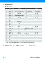
Leave open Sense pin and option detect Connect to option resistor* Leave open Sense pin and option detect Connect to option resistor* Leave open Supply ground Alternative function: Debug CLK Leave open Alternative function: Debug DATA Leave open Leave open Leave open Leave open Leave open Leave open * Option resistor should always be fitted even if channel is unused and Cs capacitor is not fixed. CMOS input and output OD CMOS open drain output
Open the catalog to page 3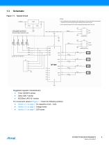
Figure 1-1. Typical Circuit NOTES: VUNREG 1) The central pad on the underside of the VQFN chip is a Vss pin and should be connected to ground. Do not put any other tracks underneath the body of the chip. 2) It is important to place all Cs and Rs components physically near to the chip. Follow regulator manufacturer's recommended values for input and output bypass capacitors (Creg). Example use of output pins SPEED SELECT Suggested regulator manufacturers: For component values in Figure 1-1 check the following sections: Section 3.1 on page 7: Cs capacitors (Cs0 – Cs3) Section 3.5 on page 7: Voltage...
Open the catalog to page 4
Introduction The AT42QT1040 (QT1040) is a digital burst mode charge-transfer (QT™) capacitive sensor driver designed for touch-key applications. The device can sense from one to four keys; one to three keys can be disabled by not installing their respective sense capacitors. Any of the four channels can be disabled in this way. The device includes all signal processing functions necessary to provide stable sensing under a wide variety of changing conditions, and the outputs are fully de-bounced. Only a few external parts are required for operation. The QT1040 modulates its bursts in a spread-spectrum...
Open the catalog to page 5
Auto Drift Compensation Signal drift can occur because of changes in Cx and Cs over time. It is crucial that drift be compensated for, otherwise false detections, non-detections, and sensitivity shifts will follow. Drift compensation is performed by making the reference level track the raw signal at a slow rate, but only while there is no detection in effect. The rate of adjustment must be performed slowly otherwise legitimate detections could be ignored. Once an object is sensed and a key is in detect, the drift compensation mechanism ceases, since the signal is legitimately high and should...
Open the catalog to page 6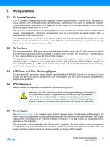
Cs Sample Capacitors Cs0 – Cs3 are the charge sensing sample capacitors; normally they are identical in nominal value. The optimal Cs values depend on the corresponding keys electrode design, the thickness of the panel and its dielectric constant. Thicker panels require larger values of Cs. Values can be in the range 2.2 nF (for faster operation) to 22 nF (for best sensitivity); typical values are 4.7 nF to 10 nF. The value of Cs should be chosen such that a light touch on a key mounted in a production unit or a prototype panel causes a reliable detection. The chosen Cs value should never be...
Open the catalog to page 7
See under Figure 1.3 on page 4 for suggested regulator manufacturers. Caution: A regulator IC shared with other logic can result in erratic operation and is not advised. A single ceramic 0.1 µF bypass capacitor, with short traces, should be placed very close to the power pins of the IC. Failure to do so can result in device oscillation, high current consumption, erratic operation, and so on. It is assumed that a larger bypass capacitor (for example, 1 µF) is somewhere else in the power circuit; for example, near the regulator. To assist with transient regulator stability problems, the QT1040...
Open the catalog to page 8
Detailed Operations Adjacent Key Suppression The use of AKS is selected by the connection of a 1 M resistor (RAKS resistor) between the SNSK0 pin and either Vdd (AKS mode on) or Vss (AKS mode off). Table 4-1. RAKS Resistor The RAKS resistor should always be connected to either Vdd or Vss and should not be changed during operation of the device. Changing the RAKS option will affect the sensitivity of the particular key. Always check that the sensitivity is suitable after a change. Retune Cs0 if necessary. Discrete Outputs There are four discrete outputs (channels 0 to 3), located on pins OUT0...
Open the catalog to page 9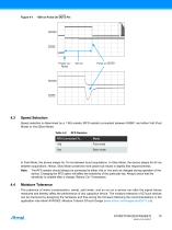
Power-on/ Reset Speed Selection Speed selection is determined by a 1 M resistor (RFS resistor) connected between SNSK1 and either Vdd (Fast Mode) or Vss (Slow Mode). Table 4-2. Fast mode Slow mode In Fast Mode, the device sleeps for 16 ms between burst acquisitions. In Slow Mode, the device sleeps for 64 ms between acquisitions. Hence, Slow Mode conserves more power but results in slightly less responsiveness. Note: The RFS resistor should always be connected to either Vdd or Vss and not changed during operation of the device. Changing the RFS option will affect the sensitivity of the particular...
Open the catalog to page 10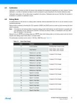
Calibration Calibration is the process by which the sensor chip assesses the background capacitance on each channel. During calibration, a number of samples are taken in quick succession to get a baseline for the channel reference value. Calibration takes place ~50 ms after power is applied to the device. Calibration also occurs if the Max On-duration is exceeded or a positive re-calibration occurs. Debug Mode An added feature to this device is a debug option whereby internal parameters from the IC can be clocked out and monitored externally. Debug mode is entered by shorting the CS3 capacitor...
Open the catalog to page 11All Atmel catalogs and technical brochures
 32-bit Microcontrollers
20 Pages
 MCUs Driving Displays
12 Pages
 Touch and 3D Gesture Control
12 Pages
 16-bit MCUs and DSCs
20 Pages
 XLP PIC® MCUs
8 Pages
 8-bit MCUs
16 Pages
 AT93C56B/66B Automotive
17 Pages
 Atmel AT86RF215 Device Family
235 Pages
 AT24C01C/02C
22 Pages
 maXTouch U Series - Flyer
2 Pages


Archived catalogs
 tinyAVR ATtiny24/44/84 Preliminary
240 Pages
 ATmega164P/324P/644P Preliminary
440 Pages
 ATmega48P/88P/168P/328P Preliminary
426 Pages
 ATmega1284P Preliminary
356 Pages
 AT90PWM216/316
359 Pages
 AT90PWM2, AT90PWM3, AT90PWM2B, AT90PWM3B
361 Pages
 ATmega329/3290/649/6490 Preliminary
392 Pages
 ATmega329P/3290P Preliminary
388 Pages
 AT90CAN32/64/128
428 Pages
 AT86RF230 Preliminary
98 Pages
 ATmega48/88/168 Automotive
335 Pages
 ATtiny25, ATtiny45, ATtiny85 Automotive
192 Pages
 ATtiny24/44/84 Automotive Preliminary
225 Pages
 AT86RF231 Preliminary
180 Pages
 Biometrics (Fingerprint Sensor)
20 Pages


- Transceiver module
- Potentiometer
- Industrial converter
- Ethernet transceiver
- Analog potentiometer
- Low-noise amplifier
- Microcontroller
- Analog amplifier
- Analog converter
- Circuit board
- Operational amplifier
- 32-bit microcontroller
- Low-power microcontroller
- Analog microcontroller
- High-speed converter
- General purpose microcontroller
- DAC converter
- Communication microcontroller
- High-speed amplifier
- ARM microcontroller