AT24C32D I2C-Compatible (2-Wire) Serial EEPROM 32-Kbit (4,096 x 8)
1 /24Pages

AT24C32D I2C-Compatible (2-Wire) Serial EEPROM 32-Kbit (4,096 x 8)
1 /24Pages
Catalog excerpts
Features Low-voltage and standard-voltage operation Internally organized as 4,096 x 8 (32K) I2C-compatible (2-Wire) serial interface Schmitt Trigger, filtered inputs for noise suppression Bidirectional data transfer protocol 400kHz (1.7V) and 1MHz (2.5V, 2.7V, 5.0V) compatibility Write Protect pin for hardware protection 32-byte Page Write mode Partial Page Writes allowed Self-timed Write cycle (5ms max) High reliability Endurance: 1,000,000 write cycles Data retention: 100 years Lead-free/Halogen-free devices available Green package options (Pb/Halide-free/RoHS compliant) 8-lead JEDEC SOIC, 8-lead TSSOP, 8-pad UDFN, 8-pad XDFN, 5-lead SOT23, 5-ball WLCSP, and 8-ball VFBGA packages Die sale options: wafer form, waffle pack, and bumped wafers Description The Atmel® AT24C32D provides 32,768 bits of Serial Electrically Erasable and Programmable Read-Only Memory (EEPROM) organized as 4,096 words of eight bits each. The device’s cascading feature allows up to eight devices to share a common 2-wire bus. The device is optimized for use in many industrial and commercial applications where low-power and low-voltage operation are essential. The devices are available in space-saving 8-lead JEDEC SOIC, 8-lead TSSOP, 8-pad UDFN, 8-pad XDFN, 5-lead SOT23, 5-ball WLCSP, and 8-ball VFBGA packages. In addition, this device operates from 1.7V to 5.5V.
Open the catalog to page 1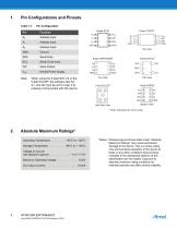
Pin Configurations and Pinouts Table 1-1. Pin Address Input Address Input Address Input Serial Data Serial Clock Input Write Protect Device Power Supply When using the 5-lead SOT-23 or the 5-ball WLCSP, the software bits A2, A1, and A0 must be set to Logic 0 to properly communicate with the device. Ball Side View Bottom View * Note: Drawings are not to scale Absolute Maximum Ratings* Operating Temperature . . . . . . . . . . .−55°C to +125°C Storage Temperature . . . . . . . . . . . −65°C to + 150°C Voltage on any pin with respect to ground . . . . . . . . . . . . . . − 1.0 V +7.0V Maximum Operating...
Open the catalog to page 2
Start Stop Logic Serial Control Logic Device Address Comparator A2 A1 A0 COMP LOAD Data Word Addr/Counter DOUT/ACK LOGIC Pin Descriptions Serial Clock (SCL): The SCL input is used to positive-edge clock data into each EEPROM device and negative-edge clock data out of each device. Serial Data (SDA): The SDA pin is bidirectional for serial data transfer. This pin is open drain driven and may be wire-ORed with any number of other open-drain or open-collector devices. Device Addresses (A2, A1, A0): The A2, A1, and A0 pins are device address inputs that are hard wired (directly to GND or to VCC) for...
Open the catalog to page 3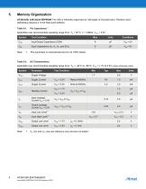
Memory Organization AT24C32D, 32K Serial EEPROM: The 32K is internally organized as 128 pages of 32-bytes each. Random word addressing requires a 12-bit data word address. Table 5-1. Applicable over recommended operating range from: TA = 25°C, f = 1.0MHz, VCC = 5.5V Symbol Test Condition This parameter is characterized and is not 100% tested. Applicable over recommended operating range from: TAI = -40°C to +85°C, VCC = 1.7V to 5.5V (unless otherwise noted). Symbol Supply Voltage Supply Current Supply Current Standby Current Input Leakage Current VCC = 5.0V Output Leakage Current VCC = 5.0V Test...
Open the catalog to page 4
AC Characteristics (Industrial Temperature) Applicable over recommended operating range from: TAI = −40°C to +85°C, VCC = 1.7V to 5.5V, CL = 100pF (unless otherwise noted). Test conditions are listed in Note 2. 1.7V Symbol Clock Pulse Width Low Clock Pulse Width High Noise Suppression Time Clock Low to Data Out Valid Time the bus must be free before a new transmission can start(1) Start Condition Hold Time Start Condition Set-up Time Data In Hold Time Data In Set-up Time Inputs Fall Time Stop Condition Set-up Time Data Out Hold Time Write Cycle Time This parameter is ensured by characterization...
Open the catalog to page 5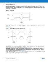
Device Operation Clock and Data Transitions: The SDA pin is normally pulled high with an external device. Data on the SDA pin may change only during SCL low time periods (See Figure 6-1). Data changes during SCL high periods will indicate a Start or Stop condition as defined below. Figure 6-1. Data Validity Data Stable Data Change Start Condition: A high-to-low transition of SDA with SCL high is a Start condition that must precede every command (See Figure 6-2). Figure 6-2. Start Condition and Stop Condition Definition Start Condition Stop Condition Stop Condition: A low-to-high transition of...
Open the catalog to page 6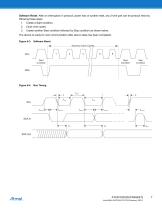
Software Reset: After an interruption in protocol, power loss or system reset, any 2-wire part can be protocol reset by following these steps: 1. Create a Start condition, Clock nine cycles, Create another Start condition followed by Stop condition as shown below. The device is ready for next communication after above steps has been completed. Figure 6-3. Software Reset Dummy Clock Cycles 1 Start Condition Start Condition Stop Condition Figure 6-4. Bus Timing tHIGH
Open the catalog to page 7
Figure 6-5. Write Cycle Timing Start Condition Stop Condition The Write cycle time tWR is the time from a valid Stop condition of a Write sequence to the end of the internal Clear/Write cycle. Figure 6-6. Output Acknowledge Start Condition
Open the catalog to page 8
Device Addressing The 32K EEPROM requires an 8-bit device address word following a Start condition to enable the chip for a Read or Write operation. The device address word consists of a mandatory ‘1010’ sequence for the first four most significant bits which is known as the device type identifier. These four bits are bit 7, bit 6, bit 5, and bit 4 as seen in Figure 7-1. This is common to all 2-wire Serial EEPROM devices. The next three bits are the A2, A1, and A0 hardware address select bits which allow as many as eight devices on the same bus. These bits must compare to their corresponding...
Open the catalog to page 9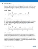
Write Operations Byte Write: A Write operation requires two 8-bit data word addresses following the device address word and acknowledgment. Upon receipt of this address, the EEPROM will again respond with a zero then clock in the first 8-bit data word. Following receipt of the 8-bit data word, the EEPROM will output a zero. The addressing device, such as a microcontroller, must then terminate the write sequence with a Stop condition. At this time, the EEPROM enters an internally-timed Write cycle, tWR, to the nonvolatile memory (See Figure 6-5). All inputs are disabled during this Write cycle...
Open the catalog to page 10All Atmel catalogs and technical brochures
 32-bit Microcontrollers
20 Pages
 MCUs Driving Displays
12 Pages
 Touch and 3D Gesture Control
12 Pages
 16-bit MCUs and DSCs
20 Pages
 XLP PIC® MCUs
8 Pages
 8-bit MCUs
16 Pages
 AT93C56B/66B Automotive
17 Pages
 Atmel AT86RF215 Device Family
235 Pages
 AT24C01C/02C
22 Pages
 maXTouch U Series - Flyer
2 Pages


Archived catalogs
 tinyAVR ATtiny24/44/84 Preliminary
240 Pages
 ATmega164P/324P/644P Preliminary
440 Pages
 ATmega48P/88P/168P/328P Preliminary
426 Pages
 ATmega1284P Preliminary
356 Pages
 AT90PWM216/316
359 Pages
 AT90PWM2, AT90PWM3, AT90PWM2B, AT90PWM3B
361 Pages
 ATmega329/3290/649/6490 Preliminary
392 Pages
 ATmega329P/3290P Preliminary
388 Pages
 AT90CAN32/64/128
428 Pages
 AT86RF230 Preliminary
98 Pages
 ATmega48/88/168 Automotive
335 Pages
 ATtiny25, ATtiny45, ATtiny85 Automotive
192 Pages
 ATtiny24/44/84 Automotive Preliminary
225 Pages
 AT86RF231 Preliminary
180 Pages
 Biometrics (Fingerprint Sensor)
20 Pages


- Transceiver module
- Potentiometer
- Industrial converter
- Ethernet transceiver
- Analog potentiometer
- Low-noise amplifier
- Analog amplifier
- Analog converter
- Circuit board
- Operational amplifier
- 32-bit microcontroller
- Low-power microcontroller
- Analog microcontroller
- High-speed converter
- General purpose microcontroller
- DAC converter
- Communication microcontroller
- High-speed amplifier
- ARM microcontroller