AT24C32D and AT24C64D I2C Automotive Temperature Serial EEPROM
1 /19Pages

AT24C32D and AT24C64D I2C Automotive Temperature Serial EEPROM
1 /19Pages
Catalog excerpts
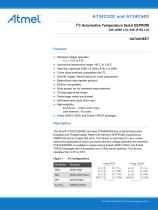
l2C Automotive Temperature Serial EEPROM • Standard-voltage operation • Automotive temperature range -40°C to 125°C • 2-wire serial interface compatible with l2C • Schmitt Trigger, filtered inputs for noise suppression • Bidirectional data transfer protocol • Write protect pin for hardware data protection • 32-byte page write modes • Partial page writes are allowed • Self-timed write cycle (5ms max) - Endurance: 1 million write cycles - Data retention: 100 years • 8-lead JEDEC SOIC and 8-lead TSSOP packages The Atmel® AT24C32D/64D provides 32768/65536 bits of Serial Electrically Erasable and Programmable Read-Only Memory (EEPROM) organized as 4096/8192 words of eight bits each. The device is optimized for use in many automotive applications where low-power and low-voltage operation are essential. AT24C32D/64D is available in space-saving 8-lead JEDEC SOIC and 8-lead TSSOP packages and is accessed via a 2-wire serial interface. This device
Open the catalog to page 1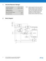
Absolute Maximum Ratings* Maximum Ratings" may cause permanent only and functional operation of the device at Voltage on any pin these Qr gny other conditions beyond those absolute maximum rating conditions for Block Diagram Data Word Data Recovery
Open the catalog to page 2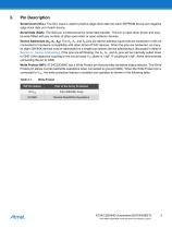
Pin Description Serial Clock (SCL): The SCL input is used to positive edge clock data into each EEPROM device and negative edge clock data out of each device. Serial Data (SDA): The SDA pin is bidirectional for serial data transfer. This pin is open-drain driven and may be wire-ORed with any number of other open-drain or open-collector devices. Device Addresses (A2, A1, A0): The A2, A1, and A0 pins are device address inputs that are hardwired or left not connected for hardware compatibility with other Atmel AT24C devices. When the pins are hardwired, as many as eight 32K/64K devices may be addressed...
Open the catalog to page 3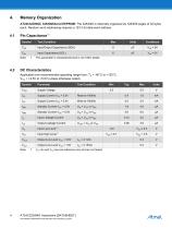
Memory Organization AT24C32D/64D, 32K/64KSerial EEPROM: The 32K/64K is internally organized as 128/256 pages of 32 bytes each. Random word addressing requires a 12/13 bit data word address. Test Condition This parameter is characterized and is not 100% tested. DC Characteristics Applicable over recommended operating range from: TA = -40°C to +125°C, VCC = +2.5V to +5.5V (unless otherwise noted). Symbol Test Condition Supply Voltage Input Leakage Current Output Leakage Current VIL min and VIH max are reference only and are not tested.
Open the catalog to page 4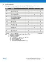
AC Characteristics Applicable over recommended operating range from TA = -40°C to +125°C, VCC = +2.5V to +5.5V, CL = 1 TTL Gate and 100pF (unless otherwise noted). Test conditions are listed in Note 3. Symbol Clock Pulse Width Low Clock Pulse Width High Clock Low to Data Out Valid Time the bus must be free before a new transmission can start(2) Start Hold Time Start Set-up Time Data In Hold Time Data In Set-up Time Stop Set-up Time Data Out Hold Time Write Cycle Time This parameter is characterized and is not 100% tested (TA = 25C). This parameter is characterized. AC measurement conditions:...
Open the catalog to page 5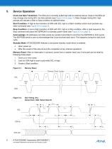
Device Operation Clock and Data Transitions: The SDA pin is normally pulled high with an external device. Data on the SDA pin may change only during SCL low time periods (see Figure 5-4 on page 7). Data changes during SCL high periods will indicate a Start or Stop condition as defined below. Start Condition: A high-to-low transition of SDA with SCL high is a Start condition which must precede any other command (see Figure 5-5 on page 7). Stop Condition: A low-to-high transition of SDA with SCL high is a Stop condition. After a read sequence, the Stop command will place the EEPROM in a standby...
Open the catalog to page 6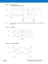
Write Cycle Timing SCL: Serial Clock, SDA: Serial Data I/O WORDn twr(1) Start Condition Stop Condition The write cycle time tWR is the time from a valid Stop condition of a write sequence to the end of the internal clear/write cycle. Data Validity Data Stable Data Change Start and Stop Definition
Open the catalog to page 7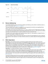
Output Acknowledge Device Addressing The 32K/64K EEPROM requires an 8-bit device address word following a start condition to enable the chip for a read or write operation (see Figure 8-1 on page 9). The device address word consists of a mandatory one, zero sequence for the first four most significant bits as shown. This is common to all the Serial EEPROM devices. The 32K/64K uses the three device address bits, A2, A1, and A0, to allow as many as eight devices on the same bus. These bits must compare to their corresponding hardwired input pins. The A2, A1, and A0 pins use an internal proprietary...
Open the catalog to page 8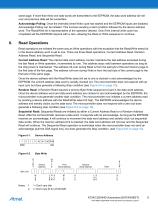
same page. If more than thirty-one data words are transmitted to the EEPROM, the data word address will rollover and previous data will be overwritten. Acknowledge Polling: Once the internally timed Write cycle has started and the EEPROM inputs are disabled, Acknowledge Polling can be initiated. This involves sending a start condition followed by the device address word. The Read/Write bit is representative of the operation desired. Only if the internal write cycle has completed will the EEPROM respond with a zero, allowing the Read or Write sequence to continue. Read Operations Read operations...
Open the catalog to page 9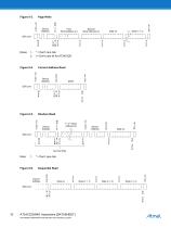
Page Write Notes: 1. * = Don't care bits Figure 8-4. Current Address Read Figure 8-5. Random Read Dummy Write Don't care bits Figure 8-6. Sequential Read
Open the catalog to page 10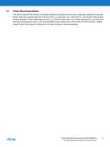
Power Recommendation The device internal POR (Power-On Reset) threshold is just below the minimum operating voltage of the device. Power shall rise monotonically from 0.0Vdc to full VCC in less than 1ms. Hold at full VCC for at least 100μs before the first operation. Power shall drop from full VCC to 0.0Vdc in less than 1ms. Power dropping to a non-zero level and then slowly going to zero is not recommended. Power shall remain off (0.0Vdc) for 0.5s minimum. Please consult Atmel if your power conditions do not meet the above recommendations.
Open the catalog to page 11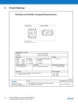
Product Markings AT24C32D and AT24C64D: Package Marking Information Note 2: Package drawings are not to scale Catalog Number Truncation AT24C32D M = Month A: January B: February ... L: December WW = Work Week of Assembly 02: Week 2 04: Week 4 ... 52: Week 52 AAA...A = Atmel Wafer Lot Number Trace Code Grade/Lead Finish Material P: Automotive/NiPdAu Atmel Truncation AT: Atmel ATM: Atmel ATML: Atmel 3/13/12 TITLE Package Mark Contact: [email protected] 24C32-64DAM, AT24C32D and AT24C64D Automotive Package Marking Information
Open the catalog to page 12All Atmel catalogs and technical brochures
 32-bit Microcontrollers
20 Pages
 MCUs Driving Displays
12 Pages
 Touch and 3D Gesture Control
12 Pages
 16-bit MCUs and DSCs
20 Pages
 XLP PIC® MCUs
8 Pages
 8-bit MCUs
16 Pages
 AT93C56B/66B Automotive
17 Pages
 Atmel AT86RF215 Device Family
235 Pages
 AT24C01C/02C
22 Pages
 maXTouch U Series - Flyer
2 Pages


Archived catalogs
 tinyAVR ATtiny24/44/84 Preliminary
240 Pages
 ATmega164P/324P/644P Preliminary
440 Pages
 ATmega48P/88P/168P/328P Preliminary
426 Pages
 ATmega1284P Preliminary
356 Pages
 AT90PWM216/316
359 Pages
 AT90PWM2, AT90PWM3, AT90PWM2B, AT90PWM3B
361 Pages
 ATmega329/3290/649/6490 Preliminary
392 Pages
 ATmega329P/3290P Preliminary
388 Pages
 AT90CAN32/64/128
428 Pages
 AT86RF230 Preliminary
98 Pages
 ATmega48/88/168 Automotive
335 Pages
 ATtiny25, ATtiny45, ATtiny85 Automotive
192 Pages
 ATtiny24/44/84 Automotive Preliminary
225 Pages
 AT86RF231 Preliminary
180 Pages
 Biometrics (Fingerprint Sensor)
20 Pages


- Transceiver module
- Potentiometer
- Industrial converter
- Ethernet transceiver
- Analog potentiometer
- Low-noise amplifier
- Microcontroller
- Analog amplifier
- Analog converter
- Circuit board
- Operational amplifier
- 32-bit microcontroller
- Low-power microcontroller
- Analog microcontroller
- High-speed converter
- General purpose microcontroller
- DAC converter
- Communication microcontroller
- High-speed amplifier
- ARM microcontroller