AT24C01C/02C
1 /22Pages

AT24C01C/02C
1 /22Pages
Catalog excerpts
Features • Low-voltage Operation - VCC = 1.7V to 5.5V • Internally Organized as 128 x 8 (1K) or 256 x 8 (2K) • I2C Compatible (2-wire) Serial Interface • Schmitt Trigger, Filtered Inputs for Noise Suppression • Bidirectional Data Transfer Protocol • 400kHz (1.7V) and 1MHz (2.5V, 2.7V, 5.0V) Compatibility • Write Protect Pin for Hardware Data Protection • 8-byte Page Write Mode - Partial Page Writes Allowed • Self-timed Write Cycle (5ms max) • High-reliability - Endurance: 1,000,000 Write Cycles - Data Retention: 100 Years • Green Package Options (Pb/Halide-free/RoHS-compliant) - 8-lead PDIP, 8-lead JEDEC SOIC, 8-lead TSSOP, 8-pad UDFN, 5-lead SOT23, and 8-ball VFBGA • Die Sale Options: Wafer Form and Tape and Reel Available Description The Atmel® AT24C01C/02C provides 1024/2048-bits of Serial Electrically Erasable and Programmable Read-Only Memory (EEPROM) organized as 128/256 words of eight bits each. Both devices include a cascading feature that allows up to eight devices to share a common 2-wire bus. These devices are optimized for use in many industrial and commercial applications where low power and low voltage operation are essential. The AT24C01C/02C are available in space saving 8-lead PDIP, 8-lead JEDEC SOIC, 8-lead TSSOP, 8-lead UDFN, 5-lead SOT23, and 8-ball VFBGA packages. In addition, the entire family operates from 1.7V to 5.5V VCC.
Open the catalog to page 1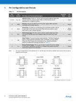
Pin Configurations and Pinouts Table 1-1. Pin Descriptions Note: 1. For use of 5-lead SOT23, the software A2, A1, and A0 bits in the device address word must be set to zero to properly communicate. Note: Package drawings are not to scale.
Open the catalog to page 2
Block Diagram Figure 2-1. Block Diagram VCC GND WP Start Stop Logic Serial Control Logic LOAD Device Address Comparator A2 A1 A0 COMP LOAD Data Word Addr/counter DOUT/ACK Logic Absolute Maximum Ratings Operating Temperature . . . . . . . . . . .-55C to +125C Storage Temperature . . . . . . . . . . . . .-65C to +150C Voltage on any pin with respect to ground . . . . . . . . . . . . . -1.0V to +7.0V Maximum Operating Voltage . . . . . . . . . . . . . . . 6.25V DC Output Current . . . . . . . . . . . . . . . . . . . . . . .5.0mA *Notice: Stresses beyond those listed under “Absolute Maximum Ratings”...
Open the catalog to page 3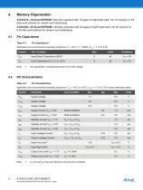
4. Memory Organization AT24C01C, 1K Serial EEPROM: Internally organized with 16 pages of eight bytes each, the 1K requires a 7-bit data word address for random word addressing. AT24C02C, 2K Serial EEPROM: Internally organized with 32 pages of eight bytes each, the 2K requires an 8-bit data word address for random word addressing. 4.1 Pin Capacitance Applicable over recommended operating range from TA = 25°C, f = 1.0MHz, VCC = 1.7V to 5.5V. Note: 1. VIL min and VIH max are reference only and are not tested.
Open the catalog to page 4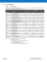
Table 4-3. AC Characteristics Applicable over recommended operating range from TAI = -40°C to +85°C, VCC = 1.7V to 5.5V, CL = 1TTL Gate and 100pF (unless otherwise noted). Test conditions are listed in Note 2. Note: 1. This parameter is ensured by characterization only. 2. AC measurement conditions: • Rl (connects to VCC): 1.3 kQ (2.5V, 5V), 10 kQ (1.7V) • Input pulse voltages: 0.3 VCC to 0.7 VCC • Input rise and fall times: < 50ns • Input and output timing reference voltages: 0.5 VCC
Open the catalog to page 5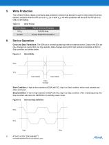
The AT24C01C/02C utilizes a hardware data protection scheme that allows the user to write protect the entire memory contents when the WP pin is at VCC (or a valid VIH). No write protection will be set if the WP pin is at GND or left floating. Table 5-1. Write Protect 6. Device Operation Clock and Data Transitions: The SDA pin is normally pulled high with an external device. Data on the SDA pin may change only during SCL low time periods. Data changes during SCL high periods will indicate a Start or Stop condition as defined below. Start Condition: A high-to-low transition of SDA with SCL high...
Open the catalog to page 6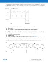
Acknowledge: All addresses and data words are serially transmitted to and from the EEPROM in 8-bit words. The EEPROM sends a zero to acknowledge that it has received each word. This happens during the ninth clock cycle. Figure 6-3. Output Acknowledge Standby Mode: The AT24C01C/02C features a low-power standby mode which is enabled: Upon power-up. After the receipt of the Stop condition and the completion of any internal operations. 2-wire Software Reset: After an interruption in protocol, power-loss, or system reset, any 2-wire part can be reset by following these steps: 1. Create a Start...
Open the catalog to page 7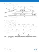
SCL: Serial Clock, SDA: Serial Data I/O tHIGH Write Cycle Timing SCL: Serial Clock, SDA: Serial Data I/O tWR Stop Condition Note: Start Condition The write cycle time tWR is the time from a valid Stop condition of a write sequence to the end of the internal clear/write cycle.
Open the catalog to page 8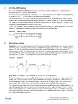
7. Device Addressing The 1-Kbit and 2-Kbit EEPROM device requires an 8-bit device address word following a Start condition to enable the device for a Read or Write operation. The device address word consists of a mandatory '1010' (0xA) sequence for the first four most significant bits as shown in Figure 7-1. This is common to all Serial EEPROM devices. The next three bits are the A2, A1, and A0 device address bits for the 1K and 2K EEPROM. These three bits must compare to their corresponding hard-wired input pins A2, A1, and A0 in order for the part to acknowledge. The eighth bit of the device...
Open the catalog to page 9
Page Write Device Address Acknowledge Polling: Once the internally timed write cycle has started and the EEPROM inputs are disabled, acknowledge polling can be initiated. This involves sending a Start condition followed by the device address word. The read/write bit is representative of the operation desired. Only if the internal write cycle has completed will the EEPROM respond with a zero allowing the read or write sequence to continue. Data Security: The AT24C01C/02C has a hardware data protection scheme that allows the user to write protect the entire memory when the WP pin is at VCC. 9....
Open the catalog to page 10All Atmel catalogs and technical brochures
 32-bit Microcontrollers
20 Pages
 MCUs Driving Displays
12 Pages
 Touch and 3D Gesture Control
12 Pages
 16-bit MCUs and DSCs
20 Pages
 XLP PIC® MCUs
8 Pages
 8-bit MCUs
16 Pages
 AT93C56B/66B Automotive
17 Pages
 Atmel AT86RF215 Device Family
235 Pages
 maXTouch U Series - Flyer
2 Pages


Archived catalogs
 tinyAVR ATtiny24/44/84 Preliminary
240 Pages
 ATmega164P/324P/644P Preliminary
440 Pages
 ATmega48P/88P/168P/328P Preliminary
426 Pages
 ATmega1284P Preliminary
356 Pages
 AT90PWM216/316
359 Pages
 AT90PWM2, AT90PWM3, AT90PWM2B, AT90PWM3B
361 Pages
 ATmega329/3290/649/6490 Preliminary
392 Pages
 ATmega329P/3290P Preliminary
388 Pages
 AT90CAN32/64/128
428 Pages
 AT86RF230 Preliminary
98 Pages
 ATmega48/88/168 Automotive
335 Pages
 ATtiny25, ATtiny45, ATtiny85 Automotive
192 Pages
 ATtiny24/44/84 Automotive Preliminary
225 Pages
 AT86RF231 Preliminary
180 Pages
 Biometrics (Fingerprint Sensor)
20 Pages


- Transceiver module
- Potentiometer
- Industrial converter
- Ethernet transceiver
- Analog potentiometer
- Low-noise amplifier
- Microcontroller
- Analog amplifier
- Analog converter
- Circuit board
- Operational amplifier
- 32-bit microcontroller
- Low-power microcontroller
- Analog microcontroller
- High-speed converter
- General purpose microcontroller
- DAC converter
- Communication microcontroller
- High-speed amplifier
- ARM microcontroller