AT17F040/080 4 and 8 Mbit In-System Programable PROM (3.3V)
1 /14Pages

AT17F040/080 4 and 8 Mbit In-System Programable PROM (3.3V)
1 /14Pages
Catalog excerpts

AT17F040 and AT17F080 FPGA Configuration Flash Memory DATASHEET Features Programmable 4,194,304 x 1 and 8,388,608 x 1-bit Serial Memories Designed to Store Configuration Programs for Field Programmable Gate Arrays (FPGAs) 3.3V Output Capability 5.0V Tolerant I/O Pins Program Support using the Atmel ATDH2200E System, ATDH2225 ISP cable, or Third-party Programmers In-System Programmable (ISP) via 2-wire Bus Simple Interface to SRAM FPGAs Compatible with Atmel AT40K and AT94K Devices, Altera® FLEX®, APEX™ Devices, Lucent® ORCA® FPGAs, Xilinx® XC3000, XC4000, XC5200, Spartan®, Virtex® FPGAs, and Motorola® MPA1000 FPGAs Cascadable Read-back to Support Additional Configurations or Higher-density Arrays Low-power CMOS FLASH Process Available in 6mm x 6mm x 1mm 8-pad LAP (Pin-compatible with 8-lead SOIC/VOIC Packages) and 20-lead PLCC Packages Emulation of the Atmel AT24C Serial EEPROMs Low-power Standby Mode Single Device Capable of Holding 4-Bitstream Files Allowing Simple System Reconfiguration Fast Serial Download Speeds up to 33MHz Endurance: 100,000 Write Cycles Typical Green (Pb/Halide-free/RoHS Compliant) Package Options Description The Atmel® AT17F Series of In-System Programmable Configuration PROMs (Configurators) provide an easy-to-use, cost-effective configuration memory solution for FPGAs. The AT17F Series devices are packaged in the 8-pad LAP and 20-lead PLCC packages (Table 1-1). The AT17F Series Configurators use a simple serial-access procedure to configure one or more FPGA devices. The AT17F Series Configurators can be programmed with industry-standard programmers, the Atmel ATDH2200E Programming Kit or the Atmel ATDH2225 ISP Cable. Table 1.
Open the catalog to page 1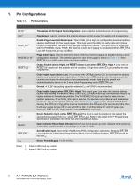
Three-state DATA Output for Configuration. Open-collector bi-directional pin for programming. Clock Input. Used to increment the internal address and bit counter for reading and programming. Enable Page Download Mode Input. When PAGE_EN is high the configuration download address space is partitioned into four equal pages. This gives users the ability to easily store and retrieve multiple configuration bitstreams from a single configuration device. This input works in conjunction with the PAGESEL inputs. PAGE_EN must be remain low if paging is not desired. When SER_EN is Low (ISP mode) this pin...
Open the catalog to page 2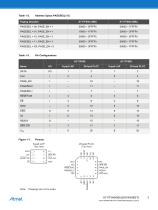
Paging Decodes
Open the catalog to page 3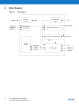
Block Diagram Figure 2-1. Block Diagram Power-on Reset Clock/Oscillator Logic Configuration Page Select Serial Download Logic Flash Memory CE/WE/OE Data Address RESET/OE SER_EN
Open the catalog to page 4
Device Description The control signals for the configuration memory device (CE, RESET/OE and CLK) interface directly with the FPGA device control signals. All FPGA devices can control the entire configuration process and retrieve data from the configuration device without requiring an external intelligent controller. The RESET/OE and CE pins control the tri-state buffer on the DATA output pin and enable the address counter. When RESET/OE is driven Low, the configuration device resets its address counter and tri-states its DATA pin. The CE pin also controls the output of the AT17F Series Configurator....
Open the catalog to page 5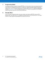
Programming Mode The programming mode is entered by bringing SER_EN Low. In this mode, the chip can be programmed by the 2-wire serial bus. The programming is done at VCC supply only. Programming super voltages are generated inside the chip. The AT17F parts are read/write at 3.3V nominal. Refer to the AT17F Programming Specification available on www.atmel.com for more programming details. AT17F devices are supported by the ATDH2200 programming system along with many third party programmers. Standby Mode The AT17F Series Configurators enter a low-power standby mode whenever SER_EN is High and...
Open the catalog to page 6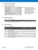
Electrical Characteristics Absolute Maximum Ratings* Operating Temperature . . . . . . . . . . . . . . . . . . . -40C to +85C Storage Temperature . . . . . . . . . . . . . . . . . . . . -65C to +150C Voltage on Any Pin with Respect to Ground . . . . . . . . . . . . . . . . .-0.1V to VCC +0.5V Supply Voltage (VCC) . . . . . . . . . . . . . . . . . . . . . . -0.5V to +4.0V Maximum Soldering Temp. (10 sec. @ 1/16in.) . . . . . . . . .260C ESD (RZAP = 1.5K, CZAP = 100pF) . . . . . . . . . . . . . . . . . . 2000V *Notice: Stresses beyond those listed under Absolute Maximum Ratings may cause permanent...
Open the catalog to page 7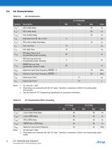
Data Hold from CE, OE, or CLK CE or OE to Data Float Delay CE Setup Time to CLK (to guarantee proper counting) CE Hold Time from CLK (to guarantee proper counting) RESET/OE Low Time (guarantees counter is reset) Maximum Input Clock Frequency SEREN = 0 Maximum Input Clock Frequency SEREN = 1 Write Cycle Time AC test load = 50pF Float delays are measured with 5pF AC loads. Transition is measured ± 200mV from steady-state active levels. See the Atmel AT17F Programming Specification for procedural information. AC Characteristics When Cascading AT17F040 CLK to Data Float Delay Maximum Input Clock...
Open the catalog to page 8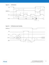
Figure 9-2. AC Waveforms when Cascading
Open the catalog to page 9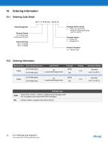
Ordering Information Ordering Code Detail AT 1 7 F 0 4 0 - 3 0 C U Package Device Grade Atmel Designator U = Green, Sn Lead Finish Industrial Temperature Range (-40°C to +85°C) Product Family 17F = FPGA Flash Configuration Memory Package Option Device Density Product Variation 30 = Default Value Ordering Information Memory Size 4-Mbit Lead Finish 8-pad, 6mm x 6mm x 1.04mm, Leadless Array Package (LAP) Pin-compatible with 8-lead SOIC/VOIC Packages 20-lead, Plastic J-leaded Chip Carrier (PLCC) Operation Range Industrial (-40C to 85C) Industrial (-40C to 85C)
Open the catalog to page 10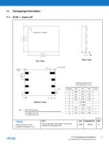
Packaging Information Side View COMMON DIMENSIONS (Unit of Measure = mm) Bottom View 1. Metal Pad Dimensions. 2. All exposed metal area shall have the following finished platings. Ni: 0.0005 to 0.015 mm Au: 0.0005 to 0.001 mm 12/22/14 TITLE Package Drawing Contact: [email protected] 8CN4, 8-pad 6x6x1.04mm Body, 1.27mm pitch Leadless Array Package (LAP)
Open the catalog to page 11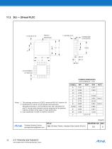
COMMON DIMENSIONS (Unit of Measure = mm) SYMBOL E Notes: 1. This package conforms to JEDEC reference MS-018, Variation AA 2. Dimensions D1 and E1 do not include mold protrusion. Allowable protrusion is .010"(0.254mm) per side. Dimension D1 and E1 include mold mismatch and are measured at the extreme material condition at the upper or lower parting line. 3. Lead coplanarity is 0.004" (0.102mm) maximum 10/04/01 Package Drawing Contact: [email protected] TITLE 20J, 20-lead, Plastic J-leaded Chip Carrier (PLCC)
Open the catalog to page 12All Atmel catalogs and technical brochures
 32-bit Microcontrollers
20 Pages
 MCUs Driving Displays
12 Pages
 Touch and 3D Gesture Control
12 Pages
 16-bit MCUs and DSCs
20 Pages
 XLP PIC® MCUs
8 Pages
 8-bit MCUs
16 Pages
 AT93C56B/66B Automotive
17 Pages
 Atmel AT86RF215 Device Family
235 Pages
 AT24C01C/02C
22 Pages
 maXTouch U Series - Flyer
2 Pages


Archived catalogs
 tinyAVR ATtiny24/44/84 Preliminary
240 Pages
 ATmega164P/324P/644P Preliminary
440 Pages
 ATmega48P/88P/168P/328P Preliminary
426 Pages
 ATmega1284P Preliminary
356 Pages
 AT90PWM216/316
359 Pages
 AT90PWM2, AT90PWM3, AT90PWM2B, AT90PWM3B
361 Pages
 ATmega329/3290/649/6490 Preliminary
392 Pages
 ATmega329P/3290P Preliminary
388 Pages
 AT90CAN32/64/128
428 Pages
 AT86RF230 Preliminary
98 Pages
 ATmega48/88/168 Automotive
335 Pages
 ATtiny25, ATtiny45, ATtiny85 Automotive
192 Pages
 ATtiny24/44/84 Automotive Preliminary
225 Pages
 AT86RF231 Preliminary
180 Pages
 Biometrics (Fingerprint Sensor)
20 Pages


- Transceiver module
- Potentiometer
- Industrial converter
- Ethernet transceiver
- Analog potentiometer
- Low-noise amplifier
- Microcontroller
- Analog amplifier
- Analog converter
- Circuit board
- Operational amplifier
- 32-bit microcontroller
- Low-power microcontroller
- Analog microcontroller
- High-speed converter
- General purpose microcontroller
- DAC converter
- Communication microcontroller
- High-speed amplifier
- ARM microcontroller