- Catalogs
- ASM Assembly Systems
- Stencils from the global No. 1
Stencils from the global No. 1
1 /20Pages

Stencils from the global No. 1
1 /20Pages
Catalog excerpts
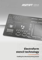
Stencils Electroform from stencil the global technology No. 1 Improving theEnabling print process the advanced and boosting printing throughput process 1
Open the catalog to page 1
Stencils from the global No.1 Stencil network Stencil technologies DEK Fine Grain stencils DEK Multi-level stencils DEK Electroform solutions DEK Electroform 3D stencils DEK Electroform variable aperture height technology (VAHT) DEK Electroform Mini LED Stencil Dek Electroform Stencil – Eform-Eco DEK PumpPrint™ / Adhesive stencils 2 | Process Support Products | Electroform Stencils fromstencil the global technology No. 1 Stencil coating technologies DEK NanoUltra Gold stencil coating NanoClear® stencil coating Smart Stencil
Open the catalog to page 2
Stencils for all your printing needs Stencil technologies As the world’s largest supplier of stencils for industrial printing processes, ASMPT is the right partner at your side. The quality of the stencil is a critical factor in the printing process. Stable and cost-effective printing processes can only be achieved with materials that are precisely manufactured and extremely resilient. ASMPT produces stencils with a wide range of technologies – from classic laser cutting to high-precision electroforming, and from single level to multi-level stencils. The broad portfolio of our award-winning stencil...
Open the catalog to page 3
Stencils from the global No. 1 ASMPT is the world’s largest manufacturer of stencils for industrial printing applications as a result of the high quality and reliability of our products and services. All of ASMPT’s factories and partners in the global stencil network operate with the same materials, the same equipment, and in accordance with strictly certified procedures. This enables us to supply our customers quickly and with consistently high quality – no matter where they may be located. Consulting Convenient ordering, fast delivery The worldwide network of ASMPT offices, service centers...
Open the catalog to page 4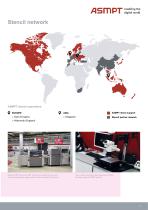
Stencil network ASMPT stencil operations EUROPE ASMPT direct support Stencil partner network Real-life SMT lines in the SMT Centers of Competence are used to provide application support and run tests including SPI analysis. Tests in labs featuring modern equipment confirm the high quality of ASMPT stencils
Open the catalog to page 5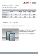
Stencil solutions – stencil technical specification LASER CUT STENCIL Standard PHD stainless steel Fine grain stainless steel Standard E-form nickel Platinum E-form stencil Wide fine grain stainless steel Hard nickel Hard nickel Material type Thickness available (µm) Thickness tolerance Area ratio window Apertures size tolerance DEK Fine Grain stencils Achieving a finer grain of stainless steel, DEK Fine Grain stencils provide superior paste release and a smoother stencil surface. DEK Fine Grain stencils can be used with the DEK Meshmounted frames, DEK VectorGuardTM Classic and DEK VectorGuardTM...
Open the catalog to page 6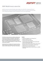
DEK Multi-level stencils Ideal for ensuring optimized solder paste height and volume for components that are distributed over a wide area, DEK Multi-level (step) stencils are produced with the latest micro-milling technology to ensure exceptional accuracy and repeatability. DEK Multi-level (step) stencils are available in stainless steel or nickel and are ideal for printing paste on SMT boards with fine pitch parts arranged over a large area. These stencils provide excellent print performance for applications with micro BGAs, 0.3 mm QFPs and small components such as 0201s metric, as well as packaging...
Open the catalog to page 7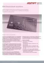
DEK Electroform solutions Achieve ultimate material volume consistency control for standard SMT, micro-SMT, semiconductor, solar and LED lighting applications with DEK Electroform stencils. Singapore Center of Competence To develop new manufacturing processes such as electroplating solutions for stencils, ASMPT operates a center of competence in Singapore with its own nickel electroplating facility. The local team has many years of experience and deep expertise in the production of electroformed stencils and parts for non-SMT components. The stencil designs are developed and tested in the adjacent...
Open the catalog to page 8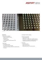
Applications: ■ Semiconductor packaging - Wafer and substrate bumping - Ball placement - Leadframe printing - Low-Temperature Co-fired Ceramics (LTCC) - Die attach ■ LED Printing - LED leadframe printing - Flux printing for flip-chip mounting - Phosphor layer printing on wafer die or over flip chip die ■ 3D printing on wafers, substrates ■ Surface-mount assembly - Standard SMT printing - VAHT stencils – variable height on different apertures - 3D stencils – print apertures on different levels; cover components and print around the covered area ■ Piece Parts - Electrical test probes - Electro-mechanical...
Open the catalog to page 9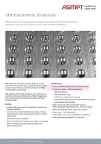
DEK Electroform 3D stencils DEK Electroform 3D stencils ensure highest print quality and throughput for jobs that require printing with different height levels and into indentations. DEK Electroform 3D stencils are single thickness stencils produced to accommodate mass imaging of surfaces that are not flat or include features or structures that would prohibit conventional one-pass printing. Well-suited for printing inside cavities or cover printing on prepopulated substrates, 3D stencils allow higher throughput and lower costs through the elimination of secondary printing or dispensing steps....
Open the catalog to page 10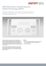
DEK Electroform Variable Aperture Height Technology (VAHT) DEK VAHT technology offers a unique alternative to multi-level stencils for nonhomogeneous assemblies that call for larger, area-specific paste volumes to accommodate bigger components. Electroform stencils can be produced with modifications to accommodate specific applications. One such adaptation is a technique called Variable Aperture Height Technology (VAHT), whereby a gasket overgrowth is created around apertures to create more aperture height to allow for increased paste volumes to be deposited. Benefits: ■ Ideal for heterogeneous...
Open the catalog to page 11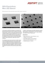
DEK Electroform Mini LED Stencil Miniaturization trend demands stencil with smaller apertures. In recent years, miniLED has emerged as a new segment with high growth potential and has drawn the interest of most major LED companies. miniLED are used in the back-light units (BLUs) of display screens and are very competitive both in terms of cost and function, offering excellent contrast though the use of local dimming. However, miniLED products pose a real problem to the packaging industry which has not yet developed solutions for handling such small dies with the accuracy and throughput required;...
Open the catalog to page 12All ASM Assembly Systems catalogs and technical brochures
 DEK TQ
4 Pages
 SIPLACE CA2
4 Pages
 DEK TQ printer platform
4 Pages
 DEK NeoHorizon iX platform
12 Pages
 IPC-HERMES-9852
2 Pages
 Galaxy Printing Platform
4 Pages
 SIPLACE X-Series S
20 Pages
 SIPLACE TX
4 Pages
 SMT Factory
6 Pages


Archived catalogs
 White Paper
20 Pages
 SIPLACE SMT-INSIGHTS
16 Pages
 SIPLACE SX
12 Pages
 ADAMOS
2 Pages
 ASM ProcessExpert
12 Pages
 Advanced Packaging
20 Pages
 SMT Smart Network
28 Pages
 SIPLACE SX-Series
12 Pages
 SIPLACE TX
4 Pages
- Automation software solution
- Measuring machine
- Process software
- Real-time software
- Control software
- Monitoring software solution
- Industrial software
- Visualization software solution
- Quality software
- Automated software
- Screen printing machine
- Reporting software
- Automatic measurement system
- Machine software
- Optical measurement system
- Automatic screen printing machine
- Planning software solution
- Control measurement system
- Centralized software
- Vertical vertical lift module