- Catalogs
- ASM Assembly Systems
- Process Lens Measure what matters – with exceptional precision, speed and stability
Process Lens Measure what matters – with exceptional precision, speed and stability
1 /4Pages

Process Lens Measure what matters – with exceptional precision, speed and stability
1 /4Pages
Catalog excerpts

ENABLING THE DIGITAL WORLD Process Lens Measure what matters – with exceptional precision, speed and stability
Open the catalog to page 1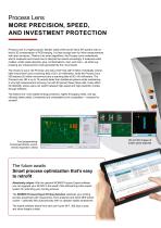
Process Lens MORE PRECISION, SPEED, AND INVESTMENT PROTECTION Process Lens is a highly precise, flexible, state-of-the-art 5D inline SPI system with onthe-fly 3D compensation of PCB warping. It is fast enough even for inline measurements with dual conveyors. Thanks to its smart algorithms, the Process Lens understands what it measures and knows how to interpret the results accordingly. It measures what matters: solder paste deposits, glue, contaminations, dust, and more – all while suppressing any measurement noise generated by the circuit board. The choice is yours: the Process Lens has a DLP...
Open the catalog to page 2
TOTALLY UNIQUE Process Lens The most Innovative measurement system Moiré phase shifting with 8 or 20 million digitally controllable micromirrors Maximum accuracy Precise X/Y positioning, combined 2D/3D measurements and on-the-fly compensation of board warpage Shadow-free Multiple light sources Comprehensive Visualization of position, area, height, volume and shape of all solder deposits; checks for coplanarity and bridging Maximum throughput Inline measurement in dual-conveyor mode Easy operation Quick programming with component library and recommendations of inspection criteria Investment protection...
Open the catalog to page 3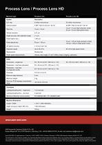
Process Lens / Process Lens HD Machine type Process Lens Camera system Pixel size 10 μm × 10 μm (high-resolution mode) 20 μm × 20 μm (high-speed mode) Vertical resolution Height accuracy with calibration target Paste deposit size Inspection speed Solder paste measurements Volume, area, height, X- and Y-offset, shape, bridging, coplanarity 70 μm × 125 μm (high-resolution mode) 130 μm × 200 μm (high-speed mode) 90 cm²/s (high-speed mode) PCBs Dimensions – single lane Dimensions – dual lane (standard) Dimensions – dual lane (in single-lane mode) Minimum edge clearance Maximum weight Maximum PCB...
Open the catalog to page 4All ASM Assembly Systems catalogs and technical brochures
 DEK TQ
4 Pages
 SIPLACE CA2
4 Pages
 DEK TQ printer platform
4 Pages
 Stencils from the global No. 1
20 Pages
 DEK NeoHorizon iX platform
12 Pages
 IPC-HERMES-9852
2 Pages
 Galaxy Printing Platform
4 Pages
 SIPLACE X-Series S
20 Pages
 SIPLACE TX
4 Pages
 SMT Factory
6 Pages


Archived catalogs
 White Paper
20 Pages
 SIPLACE SMT-INSIGHTS
16 Pages
 SIPLACE SX
12 Pages
 ADAMOS
2 Pages
 ASM ProcessExpert
12 Pages
 Advanced Packaging
20 Pages
 SMT Smart Network
28 Pages
 SIPLACE SX-Series
12 Pages
 SIPLACE TX
4 Pages
- Automation software solution
- Management software solution
- Measuring machine
- Process software
- Real-time software
- Control software
- Monitoring software solution
- Industrial software
- Visualization software solution
- Quality software
- Automated software
- Network software
- Screen printing machine
- Reporting software
- Automatic measurement system
- Machine software
- Optical measurement system
- Mounting machine
- Automatic screen printing machine
- Forming machine