- Catalogs
- ASM Assembly Systems
- Advanced Packaging
Advanced Packaging
1 /20Pages

Advanced Packaging
1 /20Pages
Catalog excerpts

WLP INSPECTION, TEST & PACKAGING End-to-end solution chains for WLSiP
Open the catalog to page 1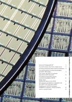
Advanced Packaging/WLSiP The whole solution chain from a single source E-forming produces the finest multi-level apertures The printing solution for advanced-packaging processes: DEK Galaxy Truly unique: SIPLACE CA combines bare-chip and SMT placement The efficient encapsulation solution in advanced packaging: ORCAS Simply clever: Molding with keep-out zone (KOZ) More precision and efficiency: Singulation with the LASER 1205 multi-beam system Finalizing your WLP/PLP processes: SUNBIRD for inspection, sorting and taping Invest in a growth market
Open the catalog to page 2
Advanced Packaging/WLSiP Separately in the past, now combined. In the past, the semiconductor - especially in back-end packaging operations - and SMT production industries operated separately from each other. In advanced packaging, their processes overlap for the first time. The result: Besides OSATs, classic electronics manufacturers can help out the semiconductor industry by supplementing its operations to meet the exploding demand for ultra-compact, SMT-capable function modules. This opens up an attractive growth market for the electronics production industry. Only at ASM: Everything from...
Open the catalog to page 3
EFORM STENCIL TECHNOLOGY Ultra-precise multi-level stencils DEK Galaxy The solution for printing and bumping DIE ATTACH & SMT SIPLACE CA Combined placement from wafers and SMT feeders The process chain for SiP applications combines classic semiconductor and SMT processes. Deposition The first process step is the deposition of flux and solder paste on the substrate. Thanks to ASM's innovative printing technologies, this can be done quickly and efficiently with the precision required for wafer-level operations. Multilevel e-formed stencils have become the standard for this process. With the additive...
Open the catalog to page 4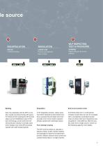
Flexible molding Precise and efficient Highly efficient all-in-one laser-cutting solution Molding Next, the substrates with the SiPs is molded, usually via press-forming with epoxy. For these and the subsequent SiP process steps such as redistribution layer in thin-layer technology, proven tools from the semiconductor industry is normally used, which explains why most SiP processes operate with wafer-shaped panels. Singulation In the singulation process, classic saws have been replaced by laser-based solutions, because they are faster and more accurate. Even more modern solutions already...
Open the catalog to page 5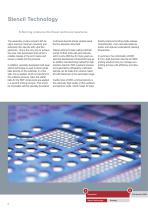
Stencil Technology E-forming produces the finest multi-level apertures The assembly of ultra-compact SiP designs requires maximum precision and extremely thin stencils with ultra-fine apertures. This is the only way to achieve the area ratio parameters that permit a reliable release of the print media and ensure a stable printing process. In addition, specially developed multi-layer stencil technology is used to place solder balls directly on the substrate. In a first step, flux is applied, which is important for the soldering process. Next, the solder balls for the SMT components are applied...
Open the catalog to page 6
Mask Photoresist Electrodeposition process Seed layer Substrate Photoresist molds Electrolytic solution Electroformed metals Metallic microstructure Source: Wikipedia ELECTROFORM STENCIL PRODUCTS SPECIFICATIONS Platinum Stencil Product Range Aperture (hole) size tolerance Aperture positional tolerance distance < 50 mm ±50 µm > 50 mm 0.1 µ/mm (VG) , 0.3 µ/mm (mesh mounted) Thickness tolerance Thickness checking Scan (presence/absence) RECOMMENDED PRINT APPLICATIONS semiconductor packaging wafer level printing LED and/or trace printing high accuracy printing multi layer stencil aperture sizes down...
Open the catalog to page 7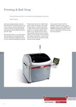
Printing & Ball Drop The printing solution for advanced packaging processes: DEK Galaxy Advanced packaging places extremely high demands on the printing process, because it requires ultra-fine apertures and maximum precision along with separate printing steps involving different technologies and media. With the DEK Galaxy, our printing experts have developed an extremely powerful, modular and flexibly configurable solution for use in advanced-packaging processes. Precise linear motors and a stable frame ensure maximum precision even at high printing speeds. In addition, ASM offers a variety of...
Open the catalog to page 8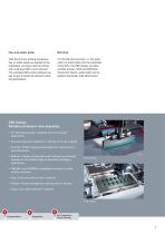
Flux and solder paste Ball drop With the first two printing processes, flux or solder paste are applied to the substrates via classic stencil printing with multi-level DEK e-form stencils. The versatile DEK printer software makes it easy to adjust all relevant operating parameters. For the ball drop process, i.e. the application of solder balls onto the underside of the SiPs, the DEK Galaxy provides another solution. With its DirEKt Ball Placement Option, solder balls can be applied individually (ball attachment). DEK Galaxy Reliable printing in chip assembly ▪ For demanding wafer, substrate...
Open the catalog to page 9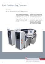
High Precision Chip Placement Truly unique: SIPLACE CA combines bare-chip and SMT placement Do you combine bare-die placement with the placement of classic SMT components in your production? Or in other words: are you looking for a universal machine that you can use to populate large carriers in panel level packaging as well as for classic SMT placement applications? These processes used to be strictly separate – until now. Today, ASM is the first equipment maker that can offer you more: the SIPLACE CA. This uniquely innovative solution tears down the borders between semiconductor backend and...
Open the catalog to page 10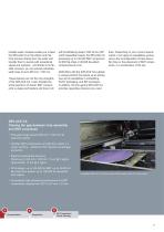
Flexible wafer modules enable you to feed the SIPLACE CA in Die Attach and Flip Chip process directly from the wafer and transfer them to panels with exceptional speed and precision. And thanks to its flexible conveyor, you can process substrate-swith sizes of up to 650 mm x 700 mm. These features are not the only strengths of the SIPLACE CA. It also handles the whole spectrum of classic SMT components via tapes and feeders and does it all with breathtaking speed. With its four SIPLACE SpeedStar heads, the SIPLACE CA processes up to 100,000 SMT component, 42,000 flip-chips or 28,000 die-attach components...
Open the catalog to page 11All ASM Assembly Systems catalogs and technical brochures
 DEK TQ
4 Pages
 SIPLACE CA2
4 Pages
 DEK TQ printer platform
4 Pages
 Stencils from the global No. 1
20 Pages
 DEK NeoHorizon iX platform
12 Pages
 IPC-HERMES-9852
2 Pages
 Galaxy Printing Platform
4 Pages
 SIPLACE X-Series S
20 Pages
 SIPLACE TX
4 Pages
 SMT Factory
6 Pages


Archived catalogs
 White Paper
20 Pages
 SIPLACE SMT-INSIGHTS
16 Pages
 SIPLACE SX
12 Pages
 ADAMOS
2 Pages
 ASM ProcessExpert
12 Pages
 SMT Smart Network
28 Pages
 SIPLACE SX-Series
12 Pages
 SIPLACE TX
4 Pages
- Automation software solution
- Measuring machine
- Process software
- Real-time software
- Control software
- Monitoring software solution
- Industrial software
- Visualization software solution
- Quality software
- Automated software
- Screen printing machine
- Reporting software
- Automatic measurement system
- Machine software
- Optical measurement system
- Automatic screen printing machine
- Planning software solution
- Control measurement system
- Centralized software
- Vertical vertical lift module