

- Products
- Catalogs
- News & Trends
- Exhibitions
VRE410

VRE410
- ±10 V output with ±1.6 mV initial accuracy.
- Temperature drift of 1.0 ppm/°C.
- Low noise level of 6 μVP-P (0.1-10 Hz).
- Tracking error of 0.3 mV.
- Excellent line regulation at 6 ppm/V typical.
- Available in a surface mount package.
The VRE410 is ideal for high precision D/A and A/D converters requiring an external precision reference and for calibrating scale factors on high-resolution A/D converters.
Description:The VRE410 is a cost-effective, high precision ±10 V reference in a 14-pin SMT package. It offers ultrastable output with a unique multipoint laser compensation technique for improved accuracy. The device features a 0.5 mV tracking error over the full operating temperature range, crucial for high-performance systems.
Selection Guide:| Model | Initial Error (mV) | Temp. Coeff. (ppm/°C) | Temp Range (°C) |
|---|---|---|---|
| VRE410AS | ±1.6 | 1.0 | 0 to +70 |
| VRE410BS | ±2.0 | 2.0 | 0 to +70 |
| VRE410JS | ±1.6 | 1.0 | -40 to +85 |
| VRE410LS | ±2.2 | 2.2 | -40 to +85 |
Power supply range is ±13.5 to ±22 V. Operating temperature ranges are 0 to +70°C for A/B models and -40 to +85°C for J/L models. The device offers continuous short circuit protection.
Theory of Operation:The VRE410 uses a 6.3 V zener diode for stability, amplified by an op amp to produce a 10 V output. A nonlinear compensation network of thermistors and resistors is used to eliminate nonlinearity in the voltage vs. temperature function, ensuring stable voltage over wide temperature ranges.
Package Options:All models are available in a 14-pin SMT DIP package.
Technical Support:For technical assistance, contact Apex Microtechnology via phone or email, or reach out to local sales representatives.
Catalog excerpts

VRE410 Precision Dual Voltage Reference FEATURES • • • • • • ±10 V Output, ± 1.6 mV Temperature Drift: 1.0 ppm/°C Low Noise: 6 μVP-P (0.1-10 Hz) Tracking Error: 0.3 mV Excellent Line Regulation: 6 ppm/V Typical Surface Mount Package APPLICATIONS The VRE410 is recommended for use as a reference for high precision D/A and A/D converters which require an external precision reference. The device is also ideal for calibrating scale factor on high resolution A/D converters. The VRE410 offers superior performance over monolithic references. DESCRIPTION The VRE410 is a low cost, high precision, ±10 V reference. Available in a 14-pin SMT package, the device is ideal for new designs that need a high performance reference. The device provides ultrastable ±10 V output with ±1.6 mV initial accuracy and a temperature coefficient of 1.0 ppm/°C. This improvement in accuracy is made possible by a unique, patented multipoint laser compensation technique. Another key feature of this reference is the 0.5 mV tracking error between the positive and negative output voltages over the full operating temperature range. This is extremely important in high performance systems for reducing overall system errors. SELECTION GUIDE Initial Error (mV) Temp. Coeff. (ppm/°C) © Apex Microtechnology Inc. All rights r
Open the catalog to page 1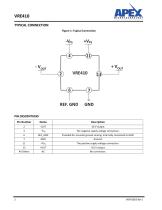
TYPICAL CONNECTION Figure 1: Typical Connection
Open the catalog to page 2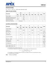
VRE410 SPECIFICATIONS VPS = +15 V, T = +25°C, RL = 10 kΩ unless otherwise noted. ABSOLUTE MAX RATINGS Parameter Power Supply Storage Temperature Short Circuit Protection ELECTRICAL SPECIFICATIONS Parameter Output Voltage Warmup Drift Long-Term Stability Output Current Line Regulation Load Regulation Power Supply Current, +PS 4 Power Supply Current, -PS 4 1. The specified values are without external trim. 2. The temperature coefficient (TC) is determined by the box method using the following formula: V MAX – V MIN 6 TC = --------------------------------------------------------------------- 10...
Open the catalog to page 3
TYPICAL PERFORMANCE GRAPHS Figure 2: VOUT vs. Temperature Figure 3: VOUTvs. Temperature
Open the catalog to page 4
Figure 6: Quiescent Current vs. Temperature Figure 7: Junction Temp Rise vs. Output Current Figure 8: PSRR vs. Frequency 120 100
Open the catalog to page 5
Figure 9: Quiescent Current vs. Figure 10: Junction Temp Rise vs. Output Current Figure 11: PSRR vs. Frequency
Open the catalog to page 6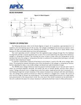
VRE410 BLOCK DIAGRAM Figure 12: Block Diagram THEORY OF OPERATION The following discussion refers to the block diagram in Figure 12. In operation, approximately 6.3 V is applied to the noninverting input of the op amp. The voltage is amplified by the op amp to produce a 10 V output. The gain is determined by the networks R1 and R2: G=1 + R2/R1. The 6.3 V zener diode is used because it is the most stable diode over time and temperature. The zener operating current is derived from the regulated output voltage through R3. This feedback arrangement provides a closely regulated zener current. This...
Open the catalog to page 7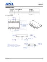
PACKAGE OPTIONS 1. Dimensions are inches & [millimeters]. 2. Bracketed alternate units are for reference only. 3. Pins: Phosphor bronze, Sn/Ag 96/4 solder dipped. 4. Material: Alumina Ceramic substrate and cover.
Open the catalog to page 9
NEED TECHNICAL HELP? CONTACT APEX SUPPORT! For all Apex Microtechnology product questions and inquiries, call toll free 800-546-2739 in North America. For inquiries via email, please contact [email protected]. International customers can also request support by contacting their local Apex Microtechnology Sales Representative. To find the one nearest to you, go to www.apexanalog.com IMPORTANT NOTICE Apex Microtechnology, Inc. has made every effort to insure the accuracy of the content contained in this document. However, the information is subject to change without notice and is provided...
Open the catalog to page 10All Apex Precision Product catalogs and technical brochures




Archived catalogs
 2008 Apex Product Summary
8 Pages
 2009 Cirrus Logic Product Summary
36 Pages
 Mixed-Signal Audio Brochure
64 Pages


- Signal amplifying integrated circuit
- Power amplifying integrated circuit
- Measuring amplifier
- Voltage amplifier
- DC amplifier
- Electronic amplifier
- High-voltage amplifier
- Low-noise amplifier
- Current amplifier
- Analog amplifier
- Adjustable amplifier
- Switching amplifier
- Current output amplifier
- Programmable amplifier
- High-power amplifier
- Operational amplifier
- Temperature amplifier
- Piezo-electric actuator amplifier
- Differential amplifier
- Linear amplifier