VRE3050
1 /13Pages

VRE3050
1 /13Pages
Catalog excerpts
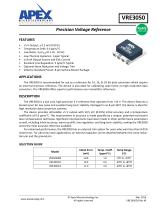
Precision Voltage Reference +5 V Output, ± 0.5 mV (0.01%) Temperature Drift: 0.6 ppm/°C Low Noise: 3 μVP-P (0.1 Hz - 10 Hz) Low Thermal Hysterisis: 1 ppm Typical ±15mA Output Source and Sink Current Excellent Line Regulation: 5 ppm/V Typical Optional Noise Reduction and Voltage Trim Industry Standard Pinout: 8-pin Surface Mount Package APPLICATIONS The VRE3050 is recommended for use as a reference for 14, 16, 0r 18 bit data converters which require an external precision reference. The device is also ideal for calibrating scale factor on high resolution data converters. The VRE3050 offers superior performance over monolithic references. DESCRIPTION The VRE3050 is a low cost, high precision 5 V reference that operates from +10 V. The device features a buried zener for low noise and excellent long term stability. Packaged in an 8-pin SMT, the device is ideal for high resolution data conversion systems. The device provides ultrastable +5 V output with ±0.5 mV (0.01%) initial accuracy and a temperature coefficient of 0.6 ppm/°C. This improvement in accuracy is made possible by a unique, patented multi-point laser compensation technique. Significant improvements have been made in other performance parameters as well, including initial accuracy, warm-up drift, line regulation, and long-term stability, making the VRE3050 series the most accurate reference available. For enhanced performance, the VRE3050 has an external trim option for users who want less than 0.01% initial error. For ultra low noise applications, an external capacitor can be attached between the noise reduction pin and the ground pin. SELECTION GUIDE Model Temp. Coeff. (ppm/ºC) © Apex Microtechnology Inc. All rights res
Open the catalog to page 1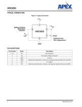
TYPICAL CONNECTION Optional Noise Figure 1: Typical Connection Optional Fine Trim Adjustment
Open the catalog to page 2
VRE3050 ELECTRICAL SPECIFICATIONS ABSOLUTE MAXIMUM RATINGS Parameter Power Supply Out, Trim Noise Reduction Operating Temp. (B) Operating Temp. (J, L) Out Short Circuit to GND Duration (VIN<12V) Out Short Circuit to GND Duration (VIN<40V) Out Short Circuit to IN Duration (VIN<12V) Continuous Power Dissipation (TA=+70°C) Storage Temperature Lead Temperature (soldering, 10 sec)
Open the catalog to page 3
VRE3050 ELECTRICAL SPECIFICATIONS VIN =+15V, T = +25°C, RL = 10 kΩ unless otherwise noted. Input Voltage Output Voltage Temperature Coefficient2 Trim Adjustment Range Turn-On Setting Time Output Noise Voltage Temperature Hysterisis Long Term Stability Supply Current ∆VOUT/ ∆IOUT The specified values are without external trim. The temperature coefficient is determined by the box method. See discussion on temperature performance. Hysterisis over the operating temperature range. Line and load regulation are measured with pulses and do not include voltage changes due to
Open the catalog to page 4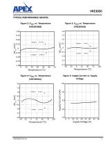
TYPICAL PERFORMANCE GRAPHS Figure 2: VOUT vs. Temperature Figure 5: Supply Current vs. Supply
Open the catalog to page 5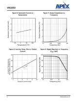
VRE3050 Figure 6: Quiescent Current vs. Temperature Figure 7: Output Impedance vs. Frequency Output Impedance Figure 8: Junction Temp. Rise vs. Output Current Figure 9: Ripple Rejection vs. Frequency (CNR =0µF)
Open the catalog to page 6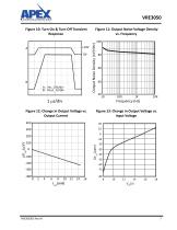
VRE3050 Figure 10: Turn-On & Turn-Off Transient Response Figure 11: Output Noise-Voltage Density vs. Frequency 100 Output Noise Density (nV Figure 12: Change in Output Voltage vs. Output Current Figure 13: Change in Output Voltage vs. Input Voltage
Open the catalog to page 7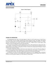
VRE3050 BLOCK DIAGRAM Figure 15: Block Diagram THEORY OF OPERATION The following discussion refers to the block diagram in Figure 15. A FET current source is used to bias a 6.3 V zener diode. The zener voltage is divided by the resistor network R1 and R2. This voltage is then applied to the non-inverting input of the operational amplifier which amplifies the voltage to produce a 5 V output. The gain is determined by the resistor networks R3 and R4: G=1 + R4/R3. The 6.3 V zener diode is used because it is the most stable diode over time and temperature. The current source provides a closely regulated...
Open the catalog to page 9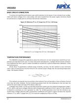
VRE3050 BASIC CIRCUIT CONNECTION To achieve the specified performance, pay careful attention to the layout. A low resistance star configuration will reduce voltage errors, noise pickup, and noise coupled from the power supply. Commons should be connected to a single point to minimize interconnect resistances. Figure 16: Reference TC vs. ∆T Change from 25°C for 1 LSB Change 10000 change from 25°C for 1 LSB change (°C) TEMPERATURE PERFORMANCE The VRE3050 is designed for applications where the initial error at room temperature and drift over temperature are important to the user. For many instrument...
Open the catalog to page 10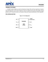
THERMAL HYSTERISIS A change in output voltage as a result of a temperature change. When references experience a tempera- ture change and return to the initial temperature, they do not always have the same initial voltage. Thermal hysterisis is difficult to correct and is a major error source in systems that experience temperature changes greater than 25°C. Reference vendors are starting to include this important specification in their datasheets.
Open the catalog to page 11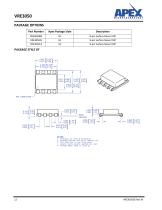
PACKAGE OPTIONS 1. Dimensions are inches & [millimeters]. 2. Bracketed alternate units are for reference only. 3. Pins: Nickel Iron, Tin over Nickel plated. 4. Material: Alumina Ceramic substrate and cover,
Open the catalog to page 12
NEED TECHNICAL HELP? CONTACT APEX SUPPORT! For all Apex Microtechnology product questions and inquiries, call toll free 800-546-2739 in North America. For inquiries via email, please contact [email protected]. International customers can also request support by contacting their local Apex Microtechnology Sales Representative. To find the one nearest to you, go to www.apexanalog.com IMPORTANT NOTICE Apex Microtechnology, Inc. has made every effort to insure the accuracy of the content contained in this document. However, the information is subject to change without notice and is provided...
Open the catalog to page 13All Apex Precision Product catalogs and technical brochures


Archived catalogs
 2008 Apex Product Summary
8 Pages
 2009 Cirrus Logic Product Summary
36 Pages
 Mixed-Signal Audio Brochure
64 Pages


- Signal amplifying integrated circuit
- Power amplifying integrated circuit
- Measuring amplifier
- Voltage amplifier
- DC amplifier
- Electronic amplifier
- High-voltage amplifier
- Low-noise amplifier
- Analog amplifier
- Current amplifier
- Adjustable amplifier
- Current output amplifier
- Switching amplifier
- Programmable amplifier
- High-power amplifier
- 2-channel amplifier
- Linear amplifier
- Temperature amplifier
- Differential amplifier