Catalog excerpts

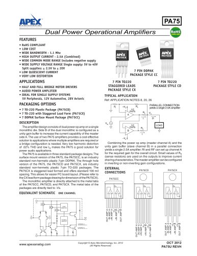
Power Operational Amplifiers FEATURES ♦ LOW COST ♦ WIDE BANDWIDTH - 1.1 Mhz ♦ HIGH OUTPUT CURRENT - 1.5A PER AMPLIFIER ♦ WIDE COMMON MODE RANGE Includes negative supply ♦ WIDE SUPPLY VOLTAGE RANGE Single supply: 5V to 40V Split supplies: ± 2.5V to ± 20V ♦ LOW QUIESCENT CURRENT ♦ VERY LOW DISTORTION The amplifier design is a dual power op amp on a single monolithic die. The quad output PA162 combines two dual op amp die in a single PSOP package. This approach provides a cost-effective solution to applications where multiple amplifiers are required or a bridge configuration is needed. Four independent amplifiers coupled with low quiescent current and very low THD makes this an ideal lowdistortion 4-channel audio amplifier for applications such as laptops and computer speakers. The quad output PA162DK is available in a surface mount 20-pin PSOP, JEDEC MO-166-AB package. Built-in thermal shutdown allows the devices to selfprotect against thermal overloads. Care must be exercised to observe the Safe Operating Area (SOA) curve and proper heatsinking will ensure maximum reliability. ♦ HALF AND FULL BRIDGE MOTOR DRIVERS ♦ AUDIO POWER AMPLIFIER Stereo - 11.3W RMS per amplifier Bridge - 22.6W RMS per two amplifiers Two Bridges - 45.2W RMS per package ♦ 3 PHASE MOTOR DRIVER 3 Channels - 33.9W RMS per package ♦ IDEAL FOR SINGLE SUPPLY SYSTEMS 5V - Peripherals 12V - Automotive 28V - Avionic ♦ PACKAGING OPTIONS 20-Pin PSOP, JEDEC MO-166-AB (PA162DK) The wide common mode input range includes the negative rail, facilitating single supply applications. This makes it possible to have a ground-based input driving a single supply amplifier with ground acting as the second or bottom supply of the amplifier. FIGURE 1. Equivalent schematic (one channel) Copyright © Apex Microtechnology, Inc. 2012 (All Rights Reserved)
Open the catalog to page 1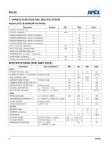
PA162 1. CHARACTERISTICS AND SPECIFICATIONS ABSOLUTE MAXIMUM RATINGS Parameter SUPPLY VOLTAGE, total OUTPUT CURRENT POWER DISSIPATION, internal (1 amplifier) POWER DISSIPATION, internal (2 amplifiers) POWER DISSIPATION, internal (3 amplifiers) POWER DISSIPATION, internal (4 amplifiers)5 INPUT VOLTAGE, differential INPUT VOLTAGE, common mode TEMPERATURE, pin solder - 10 secs max. TEMP RANGE STORAGE OPERATING TEMP RANGE, case2 SPECIFICATIONS (PER AMPLIFIER) Parameter INPUT OFFSET VOLTAGE, initial OFFSET VOLTAGE, vs. temperature Full temp range BIAS CURRENT, initial COMMON MODE RANGE Full temp...
Open the catalog to page 2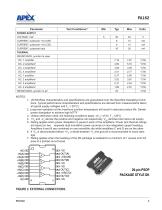
CURRENT, quiescent total POWER SUPPLY VOLTAGE, Vss4 THERMAL RESISTANCE, junction to case DC, 1 amplifier NOTES: 1. (All Min/Max characteristics and specifications are guaranteed over the Specified Operating Conditions. Typical performance characteristics and specifications are derived from measurements taken at typical supply voltages and TC = 25°C). 2. Long term operation at the maximum junction temperature will result in reduced product life. Derate power dissipation to achieve high MTTF. 3. Unless otherwise noted, the following conditions apply: ±VS = ±15V, T C =25°C. 4. +VS and -VS...
Open the catalog to page 3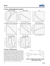
PA162 TYPICAL PERFORMANCE GRAPHS TOTAL SUPPLY VOLTAGE, V PHASE MARGIN vs. OUTPUT LOAD CAPACITANCE PULSE RESPONSE OUTPUT VOLTAGE SWING TYPICAL APPLICATION R1 and R2 set up Amplifier A as non-inverting. Amplifier B is set up as a unity gain inverter driven from the output of Amplifier A. Note that Amplifier B inverts the signals about the reference node, which is set at midsupply by R5 and R6. When the command input is midrange, so is the output of Amplifier A. Since this is also equivalent to the reference node voltage, the output of Amplifier B is the same resulting in 0V across the motor....
Open the catalog to page 4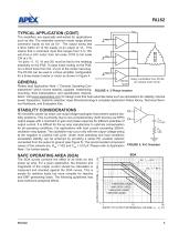
PA162 TYPICAL APPLICATION (CONT) The amplifiers are especially well-suited for applications such as this. The extended common mode range allows command inputs as low as 0V. The output swing lets it drive within 2V of the supply at an output of 1A. This means that a command input that ranges from 0 to 10V will drive a 24V motor from full scale CCW to full scale CW at ±1A. -Vs (pins 11, 15, 16 and 20) must be tied to the heatslug externally on the PCB. To ease metal routing on the PCB, run a direct trace from the -Vs pin to the center heat slug. The PA162 can be used in a three amplifier...
Open the catalog to page 5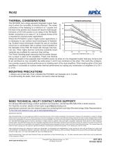
INTERNAL POWER DISSIPATION, P (W) POWER DERATING 50 The PA162DK has a large exposed integrated copper heat(A +B slug to which the monolithic is directly attached. The solder +C +D connection of the heatslug to a minimum of 1 square inch )A (A+ 40 MP B+ C) LIF foil area of the printed circuit board will result in thermal perAM IE PL RS formance of 25°C/W junction to air rating of the PA162DK. IFI LO ER 30 A SL Solder connection to an area of 1 to 2 square inches of foil OA DED (A+ DE B) A is required for minimal power applications. D MP LIF IER Where the PA162DK is used in higher power...
Open the catalog to page 6All Apex Precision Product catalogs and technical brochures
-
MP103
13 Pages
-
VRE305
9 Pages
-
VRE3050
13 Pages
-
VRE410
10 Pages
-
VRE310
9 Pages
-
VRE306
7 Pages
-
VRE107
4 Pages
-
VRE104
5 Pages
-
VRE102
10 Pages
-
SWR200
11 Pages
-
PA75
5 Pages
-
PA74 / PA76
5 Pages
-
PA162
6 Pages
-
PA02
14 Pages
-
PA16
7 Pages
-
Product Summary Guide 2013
8 Pages
Archived catalogs
-
2008 Apex Product Summary
8 Pages
-
2009 Cirrus Logic Product Summary
36 Pages
-
Mixed-Signal Audio Brochure
64 Pages


