

- Products
- Catalogs
- News & Trends
- Exhibitions
PA16

PA16
- High power bandwidth of 350kHz
- High slew rate of 20V/μs
- Fast settling time of 600ns
- Low crossover distortion in Class A/B
- Low internal losses of 1.2V at 2A
- High output current of ±5A peak
- Low input bias current with FET input
- Isolated case with 300 VDC
- Motor, valve, and actuator control
- Magnetic deflection circuits up to 5A
- Power transducers up to 350 kHz
- Audio amplifiers up to 44W RMS
The PA16 and PA16A are wideband, high output current operational amplifiers designed for driving resistive, inductive, and capacitive loads. They feature a complementary "collector output" stage that swings close to the supply rails and is protected against inductive kickback. The output stage is biased for class A/B operation for optimal linearity. The amplifiers are internally compensated but not recommended for use as unity gain followers. Continuous operation under load requires mounting on a properly rated heatsink.
- Supply Voltage: ±38V
- Output Current: 5A within SOA
- Power Dissipation: 62.5W
- Input Voltage Differential: ±30V
- Operating Temperature Range: -40°C to 85°C
These ratings include supply voltage, output current, power dissipation, input voltage, and temperature limits. Exceeding these limits may result in reduced product life.
The PA16 is suitable for vehicular sound system power stages, utilizing its low internal loss and low distortion for a clear audio amplifier. The circuit uses AC coupling to minimize DC voltage across the speaker, with current limit resistors for protection against output short circuits.
The SOA curves illustrate the limits for the power operational amplifier. For reactive and EMF generating loads, the current limits should be set appropriately to ensure safe operation.
The case is electrically isolated and should be mounted directly to a heatsink with thermal compound. Proper mounting ensures reliable operation and minimizes thermal resistance.
For technical assistance, contact Apex Microtechnology support via phone or email. International customers can reach out to local sales representatives.
Catalog excerpts
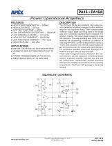
Power Operational Amplifiers FEATURES The PA16 and PA16A are wideband, high output current operational amplifiers designed to drive resistive, inductive and capacitive loads. Their complementary “collector output” stage can swing close to the supply rails and is protected against inductive kickback. For optimum linearity, the output stage is biased for class A/B operation. The safe operating area (SOA) can be observed for all operating conditions by selection of user programmable, current limiting resistors (down to 10mA). Both amplifiers are internally compensated but are not recommended for use as unity gain followers. For continuous operation under load, mounting on a heatsink of proper rating is recommended. These hybrid integrated circuits utilize thick film (cermet) resistors, ceramic capacitors and semiconductor chips to maximize reliability, minimize size and give top performance. Ultrasonically bonded aluminum wires provide reliable interconnections at all operating temperatures. The Power SIP package is electrically isolated. ♦ HIGH POWER BANDWIDTH — 350kHz ♦ HIGH SLEW RATE — 20V/μs ♦ FAST SETTLING TIME — 600ns ♦ LOW CROSSOVER DISTORTION — Class A/B ♦ LOW INTERNAL LOSSES — 1.2V at 2A ♦ HIGH OUTPUT CURRENT — ±5A PEAK ♦ LOW INPUT BIAS CURRENT — FET Input ♦ ISOLATED CASE — 300 VDC ♦ MOTOR, VALVE AND ACTUATOR CONTROL ♦ MAGNETIC DEFLECTION CIRCUITS UP TO 5A ♦ POWER TRANSDUCERS UP TO 350 kHz ♦ AUDIO AMPLIFIERS UP TO 44W RMS Copyright © Apex Microtechnology, Inc. 2
Open the catalog to page 1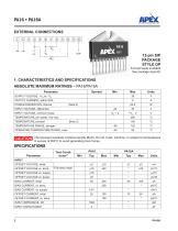
Formed leads available See package style EE 1. CHARACTERISTICS AND SPECIFICATIONS ABSOLUTE MAXIMUM RATINGS – PA16/PA16A Parameter OUTPUT CURRENT, within SOA POWER DISSIPATION, internal INPUT VOLTAGE, differential INPUT VOLTAGE, common mode TEMPERATURE, pin solder, 10s max. TEMPERATURE, junction TEMPERATURE RANGE, storage OPERATING TEMPERATURE RANGE, case The exposed substrate contains beryllia (BeO). Do not crush, machine, or subject to temperatures in excess of 850°C to avoid generating toxic fumes. SPECIFICATIONS Parameter INPUT OFFSET VOLTAGE, initial OFFSET VOLTAGE vs. temp Full temp range...
Open the catalog to page 2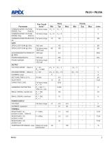
COMMON MODE VOLTAGE RANGE, Pos. (Note 6) Full temp range COMMON MODE VOLTAGE RANGE, Neg. (Note 6) Full temp range COMMON MODE REJECTION, Full temp range DC GAIN OPEN LOOP GAIN @ 10Hz OPEN LOOP GAIN @ 10Hz Full temp range, 10KΩ load GAIN BANDWIDTH PRODUCT 10Ω load @ 1MHz POWER BANDWIDTH PHASE MARGIN Full temp range, 10Ω load OUTPUT VOLTAGE SWING VOLTAGE SWING CURRENT, peak SETTLING TIME to 0.1% SLEW RATE CAPACITIVE LOAD Full temp range, A V > 10 HARMONIC DISTORTION SMALL SIGNAL rise/fall time SMALL SIGNAL overshoot POWER SUPPLY VOLTAGE Full temp range CURRENT, quiescent THERMAL RESISTANCE, AC,...
Open the catalog to page 3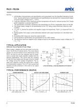
PA16 • PA16A NOTES: 1. (All Min/Max characteristics and specifications are guaranteed over the Specified Operating Conditions. Typical performance characteristics and specifications are derived from measurements taken at typical supply voltages and TC = 25°C). 2. Long term operation at the maximum junction temperature will result in reduced product life. Derate power dissipation to achieve high MTTF. * The specification of PA16A is identical to the specification for PA16 in applicable column to the left. 3. The power supply voltage for all specifications is the TYP rating unless otherwise noted...
Open the catalog to page 4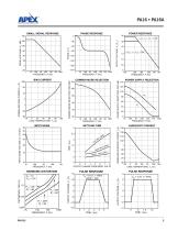
SMALL SIGNAL RESPONSE PHASE RESPONSE POWER RESPONSE BIAS CURRENT COMMON MODE REJECTION, CMR (dB) INPUT NOISE COMMON MODE REJECTION SETTLING TIME HARMONIC DISTORTION POWER SUPPLY REJECTION QUIESCENT CURRENT PULSE RESPONSE POWER SUPPLY REJECTION, PSR (dB) NORMALIZED QUIESCENT CURRENT IQ (X) OPEN LOOP GAIN, AOL (dB) NORMALIZED BIAS CURRENT, IB (X) INPUT NOISE VOLTAGE, eN (nV/√Hz) SATURATION VOLTAGE, INTERNAL POWER DISSIPA
Open the catalog to page 5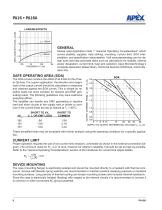
OUTPUT VOLTAGE, DELTA GAIN WITH LOAD, ∆A (dB) LOADING EFFECTS Please read Application Note 1 "General Operating Considerations" which covers stability, supplies, heat sinking, mounting, current limit, SOA interpretation, and specification interpretation. Visit www.apexanalog.com for design tools that help automate tasks such as calculations for stability, internal power dissipation, current limit; heat sink selection; Apex Microtechnology’s complete Application Notes library; Technical Seminar Workbook; and Evaluation Kits. The SOA curves combine the effect of all limits for this Power Op Amp....
Open the catalog to page 6
NEED TECHNICAL HELP? CONTACT APEX SUPPORT! For all Apex Microtechnology product questions and inquiries, call toll free 800-546-2739 in North America. For inquiries via email, please contact [email protected]. International customers can also request support by contacting their local Apex Microtechnology Sales Representative. To find the one nearest to you, go to www.apexanalog.com IMPORTANT NOTICE Apex Microtechnology, Inc. has made every effort to insure the accuracy of the content contained in this document. However, the information is subject to change without notice and is provided...
Open the catalog to page 7All Apex Precision Product catalogs and technical brochures




Archived catalogs
 2008 Apex Product Summary
8 Pages
 2009 Cirrus Logic Product Summary
36 Pages
 Mixed-Signal Audio Brochure
64 Pages


- Signal amplifying integrated circuit
- Power amplifying integrated circuit
- Measuring amplifier
- Voltage amplifier
- DC amplifier
- Electronic amplifier
- High-voltage amplifier
- Low-noise amplifier
- Current amplifier
- Analog amplifier
- Adjustable amplifier
- Switching amplifier
- Current output amplifier
- Programmable amplifier
- High-power amplifier
- Temperature amplifier
- Piezo-electric actuator amplifier
- Differential amplifier
- Linear amplifier