

- Products
- Catalogs
- News & Trends
- Exhibitions
MP103

MP103
- Supply Voltage: +VS to -VS up to 200V, -VS up to -30V, +VAUX up to 30V.
- Output Current: Peak per channel is 15A.
- Power Dissipation: 35W per channel.
- Temperature Range: Storage from -40°C to 105°C, junction up to 150°C.
- Offset Voltage: ±2mV typical.
- Bias Current: ±3.3µA typical.
- Gain: Fixed at 65 V/V with feedback connected to VOUT.
- Gain Bandwidth: 230 kHz.
- Voltage Swing: +VS - 15V to +VS - 9V for IO = 10A.
- Quiescent Current: -VS 19-26mA, +VAUX 13.5-15mA, +VS 1-5mA.
- Resistance, junction to case: 1.5-1.75°C/W for AC, 3.1-3.6°C/W for DC.
- Resistance, junction to air: 12.5-14°C/W.
- Use bypass capacitors close to power supply terminals to prevent oscillation.
- Connect current limit resistor (RLIM) as shown in diagrams for proper operation.
- Use unidirectional zener diode transient suppressors for power supply protection.
- Include a series isolation resistor for stability with capacitive loads.
Catalog excerpts
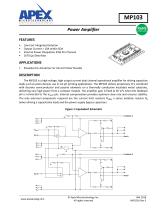
Power Amplifier Low Cost Integrated Solution Output Current > 10A within SOA Internal Power Dissipation 35W Per Channel 167V/µs Slew Rate Piezoelectric Actuation For Ink Jet Printer Nozzles DESCRIPTION The MP103 is a high voltage, high output current dual channel operational amplifier for driving capacitive loads such as piezo devices use in ink jet printing applications. The MP103 utilizes proprietary IC’s combined with discrete semiconductor and passive elements on a thermally conductive insulated metal substrate, delivering very high power from a compact module. The amplifier gain is fixed at 65 V/V when the feedback pin is connected to the VOUT pin. Internal compensation provides optimum slew rate and ensures stability. The only external components required are the current limit resistors RLIM, a series isolation resistor RS (when driving a capacitative load) and the power supply bypass capacitors. Figure 1: Equivalent Schematic Feedback A +VS +VS +VS IL IL © Apex Microtechnology Inc. All rights reserved
Open the catalog to page 1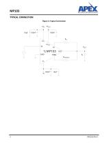
MP103 TYPICAL CONNECTION Figure 2: Typical Connection +V S +V AUX 10μF
Open the catalog to page 2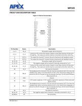
AP^C MICROTECHNOLOGY PRECISION-PONER-ANALOG PINOUT AND DESCRIPTION TABLE +Vs_A +Vs_A +Vs_A cl_a cl_a cl_a NC out_a NC NC NC NC NC NC OUT_B NC NC +Vs_B +Vs_B +Vs_B
Open the catalog to page 3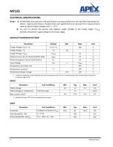
AP^X MICROTECHNOLOGY PRECISION'POWER'ANALO ELECTRICAL SPECIFICATIONS Notes: a) All Min/Max characteristics and specifications are guaranteed over the Specified Operating Conditions. Typical performance characteristics and specifications are derived from measurements taken at typical supply voltages and Tc = 25°C. b) +Vs and -Vs denote the positive and negative supply voltages to the output stages. +Vaux denotes the positive supply voltage to the input stages. ABSOLUTE MAXIMUM RATINGS
Open the catalog to page 4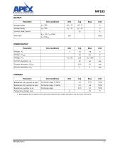
AP^C OUTPUT 1. Rating applies if the output current alternates between both output transistors at a rate faster than 60 Hz.
Open the catalog to page 5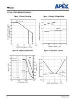
MP103 TYPICAL PERFORMANCE GRAPHS Figure 4: Power Derating Figure 5: Output Voltage Swing Voltage Drop From Supply (V) Figure 6: Frequency Response Figure 7: Quiescent Current 30 Normalized Quiescent Current, IQ (X)
Open the catalog to page 6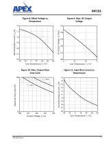
MP103 Figure 8: Offset Voltage vs. Temperature Figure 9: Max. DC Output Voltage 150 Normalized Bias Current, IB (X) Normalized Bias Current, IB (X) Maximum Duty Cycle (%) Figure 11: Input Bias Current vs. Temperature Figure 10: Max. Output Pulse Duty Cycle
Open the catalog to page 7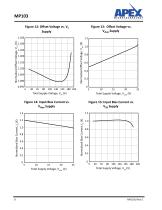
MP103 Figure 12: Offset Voltage vs. Vs Supply Figure 13: Offset Voltage vs. VAux Supply (X) Total Supply Voltage, VSS (V) Figure 15: Input Bias Current vs. VSS Supply 1.2 Normalized Bias Current, IB (X) Normalized Bias Current, IB (X) Total Supply Voltage, VAUX (V) Figure 14: Input Bias Current vs. VAux Supply Total Supply Voltage, VAUX (V) Total Supply Voltage, VSS (V)
Open the catalog to page 8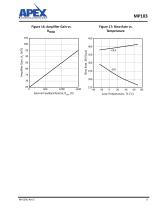
MP103 Figure 16: Amplifier Gain vs. RFDBK Figure 17: Slew Rate vs. Temperature External Feedback Resistor, RFDBK
Open the catalog to page 9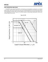
MP103 SAFE OPERATING AREA (SOA) The MOSFET output stage of the MP103 is not limited by second breakdown considerations as in bipolar output stages. Only thermal considerations and current handling capabilities limit the SOA (see Safe Operating Area graph). The output stage is protected against transient flyback by the parasitic body diodes of the output stage MOSFET structure. However, for protection against sustained high energy flyback, external fastrecovery diodes must be used. Figure 18: SOA
Open the catalog to page 10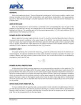
MP103 GENERAL Please read Application Note 1 “General Operating Considerations” which covers stability, supplies, heat sinking, mounting, current limit, SOA interpretation, and specification interpretation. Visit www.apexanalog.com for Apex Microtechnology’s complete Application Notes library, Technical Seminar Workbook, and Evaluation Kits. AMPLIFIER GAIN When the feedback pin for each channel is connected to the corresponding OUT pin, the gain of the amplifier is internally set to 65 V/V. The amplifier gain can be increased by connecting a resistor between the feedback and Out pin. The amplifier...
Open the catalog to page 11
MP103 BACKPLATE GROUNDING The substrate of the MP103 is an insulated metal substrate. It is required that it be connected to signal ground. This is accomplished when the ground pin (Pin 32) is properly connected to signal ground.
Open the catalog to page 12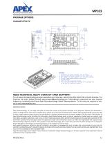
MP103 PACKAGE OPTIONS PACKAGE STYLE FC NOTES: 1. Dimensions are inches; alternate units are [mm]. 2. Recommended PCB hole diameter for pins: .050 [1.27]. 3. 2oz. copper over 600V dielectric over aluminum substrate. 4. Tin over nickel plated phosphor bronze pins. 6. Mount with #4 or equivalent screws. 7. It is not recommended that mounting of the package rely on the pins for mechanical support. NEED TECHNICAL HELP? CONTACT APEX SUPPORT! For all Apex Microtechnology product questions and inquiries, call toll free 800-546-2739 in North America. For inquiries via email, please contact [email protected]....
Open the catalog to page 13All Apex Precision Product catalogs and technical brochures




Archived catalogs
 2008 Apex Product Summary
8 Pages
 2009 Cirrus Logic Product Summary
36 Pages
 Mixed-Signal Audio Brochure
64 Pages


- Signal amplifying integrated circuit
- Measuring amplifier
- Voltage amplifier
- DC amplifier
- Electronic amplifier
- High-voltage amplifier
- Low-noise amplifier
- Current amplifier
- Analog amplifier
- Adjustable amplifier
- Switching amplifier
- Current output amplifier
- Programmable amplifier
- High-power amplifier
- Temperature amplifier
- Piezo-electric actuator amplifier
- Differential amplifier
- Linear amplifier