Catalog excerpts

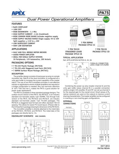
PA22 High Voltage Power Operational Amplifiers Up to ±110 V Power Supply 12 A Continuous Output Current, Typical 250 W Continuous Power Dissipation at TC = 25 oC 4 MHz Gain Bandwidth Product Programmable Voltage or Current Sources Piezo Electric Positioning Deformable Mirror Focus Electrostatic Transducers DESCRIPTION The PA22 linear power operational amplifier is specifically designed for high pulse current applications. With its peak current capability of 13.6 A and internal power dissipation of 250 W, this amplifier offers power density yet unseen in SIP form-factors. Its novel design allows for easy and reliable connection to a heatsink, as well as strong performance even when socketed. This amplifier is equipped with temperature sensing and current limit. © Apex Microtechnology Inc. All rights reserved
Open the catalog to page 1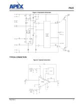
PA22 Figure 1: Equivalent Schematic +V S Current Limit Control TYPICAL CONNECTION Figure 2: Typical Connection RF +V S *Use 10 F per Amp of output current RLIM TMPL TMPH
Open the catalog to page 2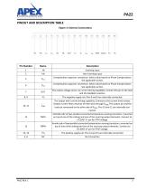
PA22 PINOUT AND DESCRIPTION TABLE Figure 3: External Connections 1 TMPL TMPH Inverting input Non-inverting input Compensation capacitor connection. Select value based on Phase Compensation. See applicable section. Compensation capacitor connection. Select value based on Phase Compensation. See applicable section. The output voltage sense, no current driving capability; connect this pin to the load and the feedback resistors. The negative supply rail. Pins 8 and 9 are internally connected. The output with current driving capability. Connect to the current limit resistor. Output current flows...
Open the catalog to page 3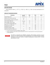
PA22 SPECIFICATIONS Unless otherwise noted: TC = 25 °C, CC = 47 pF, +VS = 100 V, -VS = -100 V. DC input specifications are +/value given. ABSOLUTE MAXIMUM RATINGS Parameter Supply Voltage, total Output Current, peak, within SOA Power Dissipation, internal, continuous2 Input Voltage, common mode ILIM to OUT Pin Voltage Differential Input Voltage, differential Temperature, pin solder, 10s Temperature, junction Temperature Range, storage Operating Temperature Range, case 1. +VS and -VS denote the positive and negative supply voltages. 2. Long term operation at the maximum junction temperature...
Open the catalog to page 4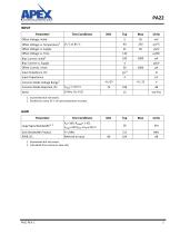
Test Conditions Bias Current, initial2 Bias Current vs. Supply Offset Current, initial Offset Voltage, initial 1 Offset Voltage vs. Temperature Offset Voltage vs. Supply Offset Voltage vs. Time Common Mode Voltage Range Common Mode Rejection, DC 1. Guaranteed but not tested. 2. Doubles for every 10 °C of case temperature increase. GAIN Parameter Test Conditions Gain Bandwidth Product PSRR, DC 1. Guaranteed but not tested. 2. Calculated from minimum slew rate.
Open the catalog to page 5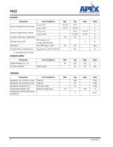
PA22 OUTPUT Parameter Output Voltage Swing, Sourcing Output Voltage Swing, Sinking Test Conditions Current, Continuous, within SOA Slew Rate 10 V step, Av=-4 2 A/µs load transient AV=-100, RLOAD = 1 kΩ Current Limit vs. Temperature POWER SUPPLY Parameter Test Conditions Current, quiescent THERMAL Parameter Resistance, AC, Junction to case Resistance, DC, junction to case Resistance, Junction to Air Temperature Range, Case Temperature Sense Diode Temp. Coefficient Test Conditions F≥60 Hz F<60 Hz Full temp range Meet full range specs
Open the catalog to page 6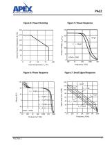
PA22 Figure 4: Power Derating Figure 5: Power Response 250 Output Voltage, VOUT(VPP) Figure 6: Phase Response Figure 7: Small Signal Response Open Loop Gain, A (dB)
Open the catalog to page 7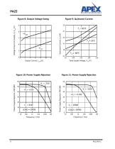
PA22 Figure 9: Quiescent Current 50 Voltage Drop From Supply, VS-VOUT(V) Figure 8: Output Voltage Swing Total Supply Voltage, VSS (V) Output Current, IOUT (A) Figure 10: Power Supply Rejection Figure 11: Power Supply Rejection
Open the catalog to page 8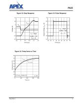
PA22 Figure 12: Step Response Figure 13: Pulse Response 15 Output Voltage, VOUT (V) Figure 14: Temp Sense vs Time 80
Open the catalog to page 9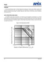
PA22 GENERAL Please read Application Note 1 “General Operating Considerations” which covers stability, supplies, heat sinking, mounting, current limit, SOA interpretation, and specification interpretation. Visit www.apexanalog.com for Apex Microtechnology’s complete Application Notes library, and Technical Seminar Workbook, and Evaluation Kits. SAFE OPERATING AREA (SOA) The MOSFET output stage of the PA22 is not limited by second breakdown considerations as in bipolar output stages. Only thermal considerations and current handling capabilities limit the SOA (see Figure 15). The output stage...
Open the catalog to page 10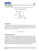
PA22 TYPICAL APPLICATION In Figure 16, PA22 is used in an inverting gain of 4 for a programmable voltage source application. Figure 16: Typical Application Schematic CURRENT LIMIT For proper operation, the current limit resistor (RLIM) must be connected as shown in the external connection diagram. For optimum reliability, the resistor value should be set as high as possible. The value is calculated as follows. The current limit function can be disabled by shorting the ILIM pin to the OUT pin. When current limit is active, an internal bias current of 20 mA typical will be shunted through...
Open the catalog to page 11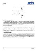
PA22 Figure 17: Overvoltage Protection +V S Z1 POWER SUPPLY BYPASSING Bypass capacitors to power supply terminals +VS and -VS must be connected physically close to the pins. Apex recommends to use electrolytic capacitors of 10 µF or greater per output amp. As additional prevention of local parasitic oscillation in the output stage of the PA22, Apex advises to place high quality ceramic capacitors (X7R) of 0.1 µF or greater in parallel to the electrolytic capacitors. PHASE COMPENSATION The external compensation capacitor CC is connected between pins 3 and 4. Unity gain stability can be...
Open the catalog to page 12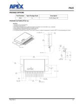
PA22 PACKAGE OPTIONS Part Number Apex Package Style PACKAGE OUTLINE (STYLE LL) NOTES: 1. Dimensions are in inches & [mm]. 2. Triangle on lid denotes Pin 1. 3. Pins: Alloy 510 phosphor bronze plated with matte tin (150-300u") over nickel (500u" max.) underplate. 4. Epoxy-sealed & ultrasonically welded non-hermetic package. 5. Creepage distance between I/O pin pads: 0.050 inches. 6. The exposed substrate contains BeO. Do not crush, machine or subject to temperatures in excess of 850 C to avoid generating toxic fumes. .0045 [.114]
Open the catalog to page 13All Apex Precision Product catalogs and technical brochures
-
MP103
13 Pages
-
VRE305
9 Pages
-
VRE3050
13 Pages
-
VRE410
10 Pages
-
VRE310
9 Pages
-
VRE306
7 Pages
-
VRE107
4 Pages
-
VRE104
5 Pages
-
VRE102
10 Pages
-
SWR200
11 Pages
-
PA75
5 Pages
-
PA74 / PA76
5 Pages
-
PA162
6 Pages
-
PA02
14 Pages
-
PA16
7 Pages
-
Product Summary Guide 2013
8 Pages
Archived catalogs
-
2008 Apex Product Summary
8 Pages
-
2009 Cirrus Logic Product Summary
36 Pages
-
Mixed-Signal Audio Brochure
64 Pages


