
- Catalogs
- Apex Precision Product
- 3000 V/µs High Voltage Power Amplifier

- Products
- Catalogs
- News & Trends
- Exhibitions
3000 V/µs High Voltage Power Amplifier

3000 V/µs High Voltage Power Amplifier
Catalog excerpts

Power Operational Amplifiers FEATURES GENERAL DESCRIPTION The PA107DP is a state of the art wideband high power operational amplifier designed to drive resistive, capacitive or inductive loads. For optimum linearity the output stage is biased for class A/B operation. Feed forward technology is used to obtain wide bandwidth and excellent DC performance, but constricts use to inverting mode only. External compensation allows the user to obtain both high gain and wide bandwidth. Use of a heatsink is required to realize the SOA. ♦ Power Bandwidth 170 VP-P, 2 MHz ♦ Output Voltage up to 180 Vp-p ♦ High Slew Rate 2500 V/µs Minimum with A CL = 20 ♦ High Gain Bandwidth Product 180 MHz ♦ High Output Current ±1.5 A Steady State Within SOA ♦ High Peak Output Current ±5 A This hybrid integrated circuit uses thick film resistors, ceramic capacitors, and semiconductors to maximize reliability, minimize size, and give top performance. Ultrasonically bonded aluminum wires provide reliable interconnections at all operating temperatures. The 12 pin SIP package occupies only 2 square inches. The use of compressible insulation washers voids the warranty. ♦ Piezo Drive ♦ CRT Beam Intensity Control ♦ ATE Applications ♦ Line Driver EQUIVALENT SCHEMATIC +VAUX Copyright © Apex Microtechnology, Inc. 2012 (All Rights Reserved)
Open the catalog to page 1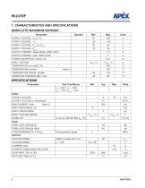
PA107DP 1. CHARACTERISTICS AND SPECIFICATIONS ABSOLUTE MAXIMUM RATINGS Parameter SUPPLY VOLTAGE, -VAUX to +VAUX SUPPLY VOLTAGE, -VAUX OUTPUT CURRENT, Steady State, (Within SOA) OUTPUT CURRENT, peak, (Within SOA) POWER DISSIPATION, internal, DC INPUT VOLTAGE TEMPERATURE, pin solder, 10s TEMPERATURE, junction TEMPERATURE RANGE, storage OPERATING TEMPERATURE, case SPECIFICATIONS Parameter Test Conditions VS = 100V, -VS = -100V, VAUX = 15V, -VAUX = -15V INPUT OFFSET VOLTAGE OFFSET VOLTAGE vs. temperature BIAS CURRENT, initial INPUT CAPACITANCE INPUT VOLTAGE RANGE NOISE, RTI GAIN OPEN LOOP GAIN @...
Open the catalog to page 2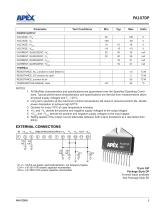
Test Conditions POWER SUPPLY VOLTAGE, +VS VOLTAGE, +VAUX VOLTAGE, -VAUX CURRENT, QUIESCENT, -VAUX CURRENT, QUIESCENT, +VAUX RESISTANCE, DC junction to case THERMAL RESISTANCE, AC, junction to case (Note 6) TEMPERATURE RANGE, case NOTES: 1. All Min/Max characteristics and specifications are guaranteed over the Specified Operating Conditions. Typical performance characteristics and specifications are derived from measurements taken at typical supply voltages and TC = 25°C. 2. Long term operation at the maximum junction temperature will result in reduced product life. Derate power dissipation to...
Open the catalog to page 3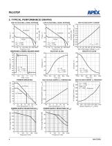
PA107DP 2. TYPICAL PERFORMANCE GRAPHS RESPONSE to 500KHz SQUARE WAVE 100 LOW VOLTAGE SMALL SIGNAL RESPONSE HIGH VOLTAGE SUPPLY CURRENT Normalized Supply Current, IQ (X) HIGH VOLTAGE SMALL SIGNAL RESPONSE POSITIVE SLEW NEGATIVE SLEW HIGH VOLTAGE CURRENT vs. FREQUENCY ±VS = ±100V ±VAUX = ±15V 10pF Load VO = 170VP-P Sinewave Power Supply Rejection (dB) POWER SUPPLY REJECTION (±VAUX) Power Supply Rejection (dB) POWER SUPPLY REJECTION (±VS) HIGH VOLTAGE CURRENT vs. TEMPERATURE POWER DERATING Internal Power Dissipation, PD (W) Normalized Quiescent Current, IQ(VS) (X)
Open the catalog to page 4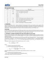
Summing Junction Input for Inverting Operational Amplifier +10V to +18V Supply for Input Circuits -10V to -18V Supply for Input Circuits +20V to +100V Supply for Gain and Gate Driver Circuits -20V to -100V Supply for Gain and Gate Driver Circuits -20V to -100V Supply for Output Source Follower High Power Output of Amplifier +20V to +100V Supply for Output Source Follower Please read Application Note 1 “General Operating Considerations” which covers stability, power supplies, heat sinking, mounting, current limit, SOA interpretation, and specification interpretation. Visit www.apexanalog.com for...
Open the catalog to page 5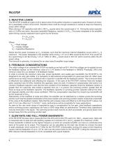
The PA107DP is stable at a gain of 20 or above when driving either inductive or capacitive loads. However an inductor is essentially a short circuit at DC, therefore there must be enough resistance in series to keep low frequency power within ratings. When driving a 1nF capacitive load with a 180 VP-P square wave, the current peak is 1 A. Driving the same capacitor with a 2.3 MHz sine wave, the power bandwidth frequency, results in 2.6 AP-P. The power dissipated in the amplifier while driving a purely capacitive load is given by the formula: Where: VPK = Peak Voltage VS = Supply Voltage XC =...
Open the catalog to page 6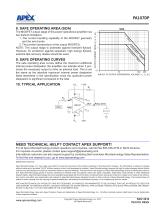
PA107DP 8. SAFE OPERATING AREA (SOA) OUTPUT CURRENT FROM +VS or -VS (A) 1 10 100 200 SUPPLY TO OUTPUT DIFFERENTIAL VOLTAGE, VS - VO (V) The safe operating area curves define the maximum additional internal power dissipation the amplifier can tolerate when it produces the necessary output to drive an external load. This is not the same as the absolute maximum internal power dissipation listed elsewhere in the specification since the quiescent power dissipation is significant compared to the total. 9. SAFE OPERATING CURVES The MOSFET output stage of this power operational amplifier has two distinct...
Open the catalog to page 7All Apex Precision Product catalogs and technical brochures




Archived catalogs
 2008 Apex Product Summary
8 Pages
 2009 Cirrus Logic Product Summary
36 Pages
 Mixed-Signal Audio Brochure
64 Pages


- Signal amplifying integrated circuit
- Power amplifying integrated circuit
- Measuring amplifier
- Voltage amplifier
- DC amplifier
- Electronic amplifier
- High-voltage amplifier
- Low-noise amplifier
- Current amplifier
- Analog amplifier
- Adjustable amplifier
- Switching amplifier
- Current output amplifier
- Programmable amplifier
- High-power amplifier
- Temperature amplifier
- Piezo-electric actuator amplifier
- Differential amplifier
- Linear amplifier